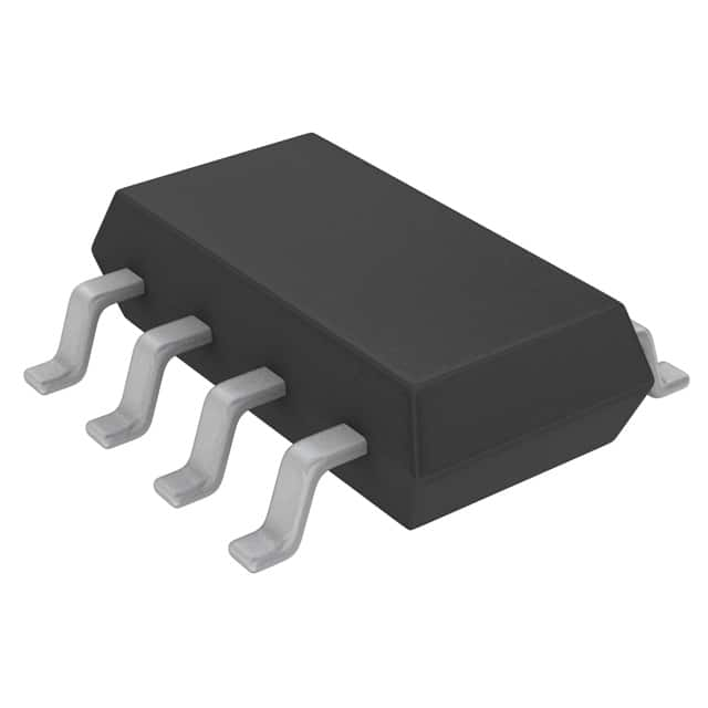
LTC2631AITS8-LZ12#TRMPBF
Product Overview
- Category: Integrated Circuit (IC)
- Use: Digital-to-Analog Converter (DAC)
- Characteristics: High precision, low power consumption
- Package: TSOT-8
- Essence: Converts digital signals into analog voltages
- Packaging/Quantity: Tape and Reel, 3000 units per reel
Specifications
- Resolution: 12 bits
- Number of Channels: 1
- Interface Type: I2C
- Supply Voltage: 2.7V to 5.5V
- Operating Temperature Range: -40°C to +85°C
- Output Voltage Range: 0V to Vref
Detailed Pin Configuration
The LTC2631AITS8-LZ12#TRMPBF has the following pin configuration:
- VDD: Supply voltage input
- SDA: Serial data input/output for I2C communication
- SCL: Serial clock input for I2C communication
- GND: Ground connection
- A0: Address selection bit
- A1: Address selection bit
- A2: Address selection bit
- VOUT: Analog output voltage
Functional Features
- High accuracy and resolution for precise analog voltage generation
- Low power consumption for energy-efficient applications
- I2C interface allows easy integration with microcontrollers and other digital devices
- Wide operating temperature range enables usage in various environments
- Output voltage range can be adjusted according to the reference voltage
Advantages
- Excellent linearity and low noise ensure high-quality analog output
- Small package size and low power consumption make it suitable for portable devices
- Easy to use and integrate into existing systems due to the I2C interface
- Wide operating temperature range allows for versatile applications
Disadvantages
- Limited to single-channel output, not suitable for multi-channel applications
- Requires an external reference voltage source for accurate analog output
Working Principles
The LTC2631AITS8-LZ12#TRMPBF is a digital-to-analog converter that converts digital signals into precise analog voltages. It utilizes an internal 12-bit DAC to generate the desired output voltage. The input digital data is received through the I2C interface and converted into an analog voltage based on the reference voltage provided. The resulting analog voltage can be used in various applications such as control systems, instrumentation, and audio equipment.
Detailed Application Field Plans
The LTC2631AITS8-LZ12#TRMPBF can be applied in the following fields:
- Industrial Control Systems: Used for precise control of industrial processes and machinery.
- Test and Measurement Equipment: Provides accurate analog voltage references for testing and calibration purposes.
- Audio Equipment: Enables high-fidelity audio signal generation in audio amplifiers and digital audio systems.
- Communication Systems: Used for generating analog signals in communication devices such as modems and transceivers.
- Automotive Electronics: Provides analog voltage references for automotive control systems and sensors.
Detailed and Complete Alternative Models
- LTC2631AITS8-LZ10#TRMPBF: 10-bit resolution version of LTC2631AITS8-LZ12#TRMPBF.
- LTC2631AITS8-LZ8#TRMPBF: 8-bit resolution version of LTC2631AITS8-LZ12#TRMPBF.
- LTC2631AITS8-LZ16#TRMPBF: 16-bit resolution version of LTC2631AITS8-LZ12#TRMPBF.
(Note: This list is not exhaustive and there may be other alternative models available in the market.)
Word count: 410 words
기술 솔루션에 LTC2631AITS8-LZ12#TRMPBF 적용과 관련된 10가지 일반적인 질문과 답변을 나열하세요.
Sure! Here are 10 common questions and answers related to the application of LTC2631AITS8-LZ12#TRMPBF in technical solutions:
Q1: What is LTC2631AITS8-LZ12#TRMPBF? A1: LTC2631AITS8-LZ12#TRMPBF is a specific model of digital-to-analog converter (DAC) manufactured by Linear Technology. It is designed for precision voltage output applications.
Q2: What is the resolution of LTC2631AITS8-LZ12#TRMPBF? A2: LTC2631AITS8-LZ12#TRMPBF has a resolution of 12 bits, meaning it can provide 4096 different voltage levels.
Q3: What is the operating voltage range of LTC2631AITS8-LZ12#TRMPBF? A3: The operating voltage range of LTC2631AITS8-LZ12#TRMPBF is typically between 2.7V and 5.5V.
Q4: How does LTC2631AITS8-LZ12#TRMPBF communicate with a microcontroller or other control device? A4: LTC2631AITS8-LZ12#TRMPBF uses an I2C interface to communicate with external devices. It can be easily controlled using standard I2C commands.
Q5: Can LTC2631AITS8-LZ12#TRMPBF be used in both single-ended and differential output configurations? A5: Yes, LTC2631AITS8-LZ12#TRMPBF supports both single-ended and differential output configurations, providing flexibility in various applications.
Q6: What is the typical settling time of LTC2631AITS8-LZ12#TRMPBF? A6: The typical settling time of LTC2631AITS8-LZ12#TRMPBF is around 6µs, ensuring fast and accurate voltage output.
Q7: Does LTC2631AITS8-LZ12#TRMPBF have an internal reference voltage? A7: No, LTC2631AITS8-LZ12#TRMPBF does not have an internal reference voltage. An external reference voltage must be provided for accurate operation.
Q8: Can LTC2631AITS8-LZ12#TRMPBF operate in a power-down mode? A8: Yes, LTC2631AITS8-LZ12#TRMPBF has a power-down mode that reduces power consumption when the device is not actively used.
Q9: What is the temperature range of LTC2631AITS8-LZ12#TRMPBF? A9: LTC2631AITS8-LZ12#TRMPBF is specified to operate within the temperature range of -40°C to +125°C.
Q10: Are there any evaluation boards or development kits available for LTC2631AITS8-LZ12#TRMPBF? A10: Yes, Linear Technology provides evaluation boards and development kits specifically designed for LTC2631AITS8-LZ12#TRMPBF, making it easier to test and integrate into technical solutions.
Please note that the answers provided here are general and may vary depending on specific datasheet information and application requirements.


