

LTC6256CDC#TRMPBF
Product Overview
Category: Integrated Circuit (IC)
Use: The LTC6256CDC#TRMPBF is a high-speed, low-power operational amplifier designed for use in various electronic applications.
Characteristics: - High speed: The LTC6256CDC#TRMPBF offers fast response times, making it suitable for applications requiring quick signal processing. - Low power consumption: This operational amplifier is designed to operate efficiently with minimal power consumption, making it ideal for battery-powered devices. - Wide supply voltage range: The LTC6256CDC#TRMPBF can operate from a wide range of supply voltages, providing flexibility in different applications. - Rail-to-rail input and output: It supports rail-to-rail input and output voltage ranges, allowing for accurate signal amplification and processing.
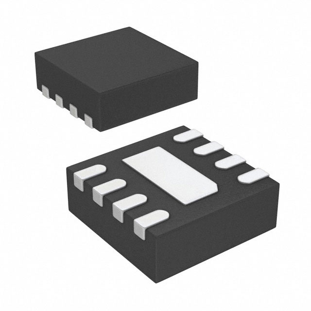
Package: The LTC6256CDC#TRMPBF comes in a small 8-pin DFN (Dual Flat No-Lead) package, which provides compactness and ease of integration into various circuit designs.
Essence: This operational amplifier is designed to provide high-speed, low-power performance for a wide range of electronic applications.
Packaging/Quantity: The LTC6256CDC#TRMPBF is typically available in reels containing a quantity of 2500 units.
Specifications
- Supply Voltage Range: 2.7V to 5.5V
- Input Offset Voltage: ±1mV (maximum)
- Gain Bandwidth Product: 100MHz
- Slew Rate: 180V/μs
- Quiescent Current: 1.3mA
- Operating Temperature Range: -40°C to 125°C
Pin Configuration
The LTC6256CDC#TRMPBF has the following pin configuration:
```
| | --| IN- V+ |-- --| IN+ OUT |-- --| V- NC |-- |___________| ```
Functional Features
- High-speed signal amplification and processing
- Low power consumption for efficient operation
- Rail-to-rail input and output voltage range for accurate signal handling
- Wide supply voltage range for flexibility in different applications
Advantages and Disadvantages
Advantages: - Fast response times enable quick signal processing. - Low power consumption makes it suitable for battery-powered devices. - Wide supply voltage range provides flexibility in various applications. - Rail-to-rail input and output allow for accurate signal amplification.
Disadvantages: - Limited availability in certain package options. - May require additional external components for specific applications.
Working Principles
The LTC6256CDC#TRMPBF operates as a high-speed operational amplifier by amplifying input signals with low power consumption. It utilizes advanced circuitry to achieve fast response times and accurate signal processing. The rail-to-rail input and output capability allows for precise amplification of signals within the specified voltage range.
Detailed Application Field Plans
The LTC6256CDC#TRMPBF can be used in a wide range of electronic applications, including: 1. Audio amplifiers 2. Data acquisition systems 3. Sensor interfaces 4. Battery-powered devices 5. Signal conditioning circuits
Detailed and Complete Alternative Models
Some alternative models that offer similar functionality to the LTC6256CDC#TRMPBF include: - AD8605 - MAX4239 - OPA2365
These alternatives can be considered based on specific application requirements and availability.
Word count: 409 words
기술 솔루션에 LTC6256CDC#TRMPBF 적용과 관련된 10가지 일반적인 질문과 답변을 나열하세요.
Sure! Here are 10 common questions and answers related to the application of LTC6256CDC#TRMPBF in technical solutions:
Q: What is LTC6256CDC#TRMPBF? A: LTC6256CDC#TRMPBF is a high-speed, low-power operational amplifier (op-amp) manufactured by Linear Technology (now part of Analog Devices). It is commonly used in various technical applications.
Q: What is the supply voltage range for LTC6256CDC#TRMPBF? A: The supply voltage range for LTC6256CDC#TRMPBF is typically between 2.7V and 5.5V.
Q: What is the typical gain bandwidth product (GBW) of LTC6256CDC#TRMPBF? A: The typical GBW of LTC6256CDC#TRMPBF is around 20 MHz.
Q: Can LTC6256CDC#TRMPBF operate with a single power supply? A: Yes, LTC6256CDC#TRMPBF can operate with a single power supply. It has rail-to-rail input and output capabilities.
Q: What is the input offset voltage of LTC6256CDC#TRMPBF? A: The input offset voltage of LTC6256CDC#TRMPBF is typically around 500 µV.
Q: Is LTC6256CDC#TRMPBF suitable for low-power applications? A: Yes, LTC6256CDC#TRMPBF is designed for low-power applications, with a typical quiescent current of around 1.6 mA.
Q: Can LTC6256CDC#TRMPBF drive capacitive loads? A: Yes, LTC6256CDC#TRMPBF has a high output current capability, allowing it to drive capacitive loads up to a certain limit.
Q: What is the input common-mode voltage range of LTC6256CDC#TRMPBF? A: The input common-mode voltage range of LTC6256CDC#TRMPBF extends from the negative supply voltage (V-) to within 1.2V of the positive supply voltage (V+).
Q: Does LTC6256CDC#TRMPBF have built-in protection features? A: Yes, LTC6256CDC#TRMPBF has built-in protection features such as thermal shutdown and reverse battery protection.
Q: Can LTC6256CDC#TRMPBF be used in precision applications? A: While LTC6256CDC#TRMPBF offers good performance, it may not be suitable for ultra-precision applications due to its input offset voltage and other non-ideal characteristics.