

MAX532AEWE+T
Product Overview
- Category: Integrated Circuit (IC)
- Use: Digital-to-Analog Converter (DAC)
- Characteristics: High precision, low power consumption
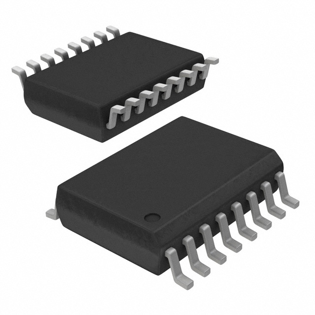
- Package: 16-pin wide SOIC (Small Outline Integrated Circuit)
- Essence: Converts digital signals into analog voltage outputs
- Packaging/Quantity: Tape and reel, 2500 units per reel
Specifications
- Resolution: 12 bits
- Number of Channels: 1
- Supply Voltage: 2.7V to 5.5V
- Operating Temperature Range: -40°C to +85°C
- Output Voltage Range: 0V to VREF
- DNL (Differential Non-Linearity): ±0.5 LSB (Least Significant Bit)
- INL (Integral Non-Linearity): ±1 LSB
- Power Consumption: 0.5mW (typical)
Pin Configuration
The MAX532AEWE+T has a total of 16 pins arranged as follows:
- VDD - Positive supply voltage
- VREF - Reference voltage input
- AGND - Analog ground
- OUT - Analog output voltage
- DGND - Digital ground
- DIN - Serial data input
- SCLK - Serial clock input
- SYNC - Synchronization input
- LDAC - Load DAC input
- CLR - Clear input
- A0 - Address input bit 0
- A1 - Address input bit 1
- A2 - Address input bit 2
- A3 - Address input bit 3
- A4 - Address input bit 4
- VSS - Negative supply voltage
Functional Features
- High-resolution digital-to-analog conversion
- Low power consumption for energy-efficient applications
- Wide operating voltage range for flexibility
- Serial interface for easy integration with microcontrollers
- Synchronization input for precise timing control
- Clear input for resetting the DAC output
- Address inputs for multiple device selection
Advantages and Disadvantages
Advantages: - High precision conversion - Low power consumption - Wide operating voltage range - Easy integration with microcontrollers - Precise timing control
Disadvantages: - Limited to single-channel output - Requires external reference voltage
Working Principles
The MAX532AEWE+T is a digital-to-analog converter that converts digital signals into analog voltage outputs. It utilizes a 12-bit resolution to provide high precision conversion. The input digital data is received through the serial data input (DIN) pin and synchronized with the serial clock input (SCLK). The converted analog voltage is available at the OUT pin. The LDAC pin allows for simultaneous updating of multiple DACs, while the CLR pin resets the output voltage. The address pins (A0-A4) enable the selection of multiple devices.
Detailed Application Field Plans
The MAX532AEWE+T can be used in various applications, including:
- Audio Systems: Providing accurate analog voltage outputs for audio signal processing.
- Instrumentation: Generating precise control voltages for measurement equipment.
- Industrial Automation: Converting digital control signals into analog outputs for industrial processes.
- Communication Systems: Producing analog signals for modulation and demodulation purposes.
- Test and Measurement: Enabling accurate voltage generation for testing electronic components.
Detailed and Complete Alternative Models
- MAX531BCPD+: Similar specifications, different package (14-pin DIP)
- MAX533BCPE+: Higher resolution (14 bits), similar package (16-pin PDIP)
- MAX534BCPE+: Higher resolution (16 bits), similar package (16-pin PDIP)
- MAX535BCPE+: Higher resolution (18 bits), similar package (16-pin PDIP)
- MAX536BCPE+: Higher resolution (20 bits), similar package (16-pin PDIP)
(Note: The above alternative models are provided for reference and may have different characteristics or availability.)
This entry provides an overview of the MAX532AEWE+T digital-to-analog converter, including its basic information, specifications, pin configuration, functional features, advantages and disadvantages, working principles, detailed application field plans, and alternative models.
기술 솔루션에 MAX532AEWE+T 적용과 관련된 10가지 일반적인 질문과 답변을 나열하세요.
Sure! Here are 10 common questions and answers related to the application of MAX532AEWE+T in technical solutions:
Question: What is the MAX532AEWE+T?
Answer: The MAX532AEWE+T is a digital-to-analog converter (DAC) IC manufactured by Maxim Integrated. It converts digital signals into analog voltages.Question: What is the operating voltage range of MAX532AEWE+T?
Answer: The operating voltage range of MAX532AEWE+T is typically between 2.7V and 5.5V.Question: What is the resolution of MAX532AEWE+T?
Answer: The MAX532AEWE+T has a resolution of 12 bits, which means it can represent 4096 different voltage levels.Question: What is the maximum output voltage range of MAX532AEWE+T?
Answer: The maximum output voltage range of MAX532AEWE+T is typically between 0V and VREF, where VREF is the reference voltage supplied to the DAC.Question: How can I interface with MAX532AEWE+T?
Answer: MAX532AEWE+T can be interfaced using a serial interface such as SPI (Serial Peripheral Interface) or I2C (Inter-Integrated Circuit).Question: Can MAX532AEWE+T operate in single-ended mode?
Answer: Yes, MAX532AEWE+T can operate in both single-ended and differential modes, depending on the application requirements.Question: What is the settling time of MAX532AEWE+T?
Answer: The settling time of MAX532AEWE+T is typically around 10µs, which is the time taken for the output voltage to reach within a specified error band after a change in the digital input.Question: Does MAX532AEWE+T have any built-in reference voltage?
Answer: No, MAX532AEWE+T does not have a built-in reference voltage. An external reference voltage needs to be provided to the VREF pin.Question: Can I use MAX532AEWE+T in battery-powered applications?
Answer: Yes, MAX532AEWE+T is suitable for battery-powered applications as it has a low operating voltage range and low power consumption.Question: What are some typical applications of MAX532AEWE+T?
Answer: MAX532AEWE+T can be used in various applications such as audio systems, instrumentation, industrial control, motor control, and communication systems where precise analog voltage generation is required.
Please note that the answers provided here are general and may vary depending on specific datasheet specifications and application requirements.