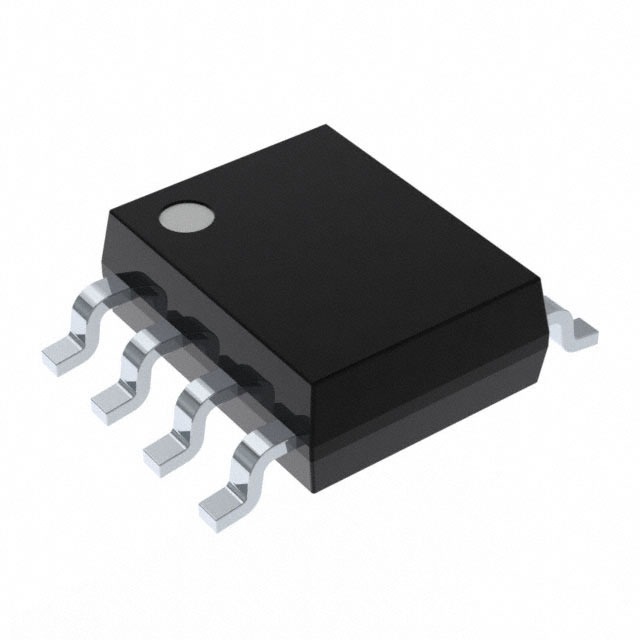
MAX749CSA
Product Overview
- Category: Integrated Circuit (IC)
- Use: Voltage Regulator
- Characteristics: Low-dropout, adjustable output voltage
- Package: Small Outline Integrated Circuit (SOIC)
- Essence: Regulates input voltage to a desired output voltage level
- Packaging/Quantity: Tape and Reel, 2500 units per reel
Specifications
- Input Voltage Range: 2.5V to 16V
- Output Voltage Range: 1.25V to 15V
- Dropout Voltage: 0.3V at 100mA load current
- Maximum Output Current: 100mA
- Line Regulation: ±0.02%/V
- Load Regulation: ±0.05%
- Quiescent Current: 80µA
- Operating Temperature Range: -40°C to +85°C
Pin Configuration
The MAX749CSA has a total of 8 pins:
- GND (Ground)
- IN (Input Voltage)
- ADJ (Adjustment Pin)
- OUT (Output Voltage)
- NC (No Connection)
- NC (No Connection)
- NC (No Connection)
- VCC (Supply Voltage)
Functional Features
- Low dropout voltage ensures efficient regulation even with low input-output differentials.
- Adjustable output voltage allows for flexibility in various applications.
- Excellent line and load regulation characteristics ensure stable output voltage under varying conditions.
- Low quiescent current minimizes power consumption.
Advantages
- Wide input voltage range enables compatibility with various power sources.
- Adjustable output voltage provides versatility for different circuit requirements.
- Small package size allows for space-saving designs.
- Low dropout voltage ensures efficient power conversion.
Disadvantages
- Limited maximum output current may restrict usage in high-power applications.
- Lack of thermal protection may pose a risk of overheating in certain conditions.
- Non-standard pin configuration may require additional attention during circuit design.
Working Principles
The MAX749CSA is a voltage regulator IC that utilizes a low-dropout architecture to regulate the input voltage to a desired output voltage level. It operates by comparing the output voltage with a reference voltage and adjusting the pass transistor accordingly. The adjustable output voltage is achieved by varying the resistance connected to the ADJ pin.
Detailed Application Field Plans
The MAX749CSA finds applications in various fields, including:
- Battery-powered devices: Provides stable voltage supply for portable electronics.
- Automotive systems: Regulates voltage for automotive sensors and control modules.
- Industrial equipment: Ensures reliable power delivery in industrial automation systems.
- Communication devices: Maintains constant voltage levels in telecommunication equipment.
- Consumer electronics: Powers audio/video equipment, gaming consoles, and other consumer devices.
Detailed and Complete Alternative Models
- LM1117-ADJ: Adjustable voltage regulator with similar specifications and pin configuration.
- LT1763-ADJ: Low dropout regulator offering adjustable output voltage and high accuracy.
- TPS7A4700: Ultra-low noise, high PSRR voltage regulator suitable for sensitive applications.
- MCP1700-ADJ: Low quiescent current LDO regulator with adjustable output voltage.
(Note: This list is not exhaustive and there are several other alternative models available in the market.)
Word count: 443 words
기술 솔루션에 MAX749CSA 적용과 관련된 10가지 일반적인 질문과 답변을 나열하세요.
Sure! Here are 10 common questions and answers related to the application of MAX749CSA in technical solutions:
Q: What is MAX749CSA? A: MAX749CSA is a high-speed, low-power comparator IC (integrated circuit) commonly used in various electronic applications.
Q: What is the operating voltage range of MAX749CSA? A: The operating voltage range of MAX749CSA is typically between 2.7V and 11V.
Q: What is the maximum output current of MAX749CSA? A: The maximum output current of MAX749CSA is approximately 20mA.
Q: Can MAX749CSA operate in both single-supply and dual-supply configurations? A: Yes, MAX749CSA can be operated in both single-supply and dual-supply configurations, depending on the application requirements.
Q: What is the typical response time of MAX749CSA? A: The typical response time of MAX749CSA is around 8ns.
Q: Can MAX749CSA tolerate overvoltage conditions? A: No, MAX749CSA is not designed to tolerate overvoltage conditions. It is recommended to use external protection circuits if overvoltage is a concern.
Q: What is the input offset voltage of MAX749CSA? A: The input offset voltage of MAX749CSA is typically around 2mV.
Q: Is MAX749CSA suitable for precision applications? A: While MAX749CSA offers good performance, it may not be ideal for precision applications due to its input offset voltage and other factors. Precision comparators are available for such applications.
Q: Can MAX749CSA be used in high-frequency applications? A: Yes, MAX749CSA can be used in high-frequency applications as it has a fast response time and good bandwidth.
Q: What are some common applications of MAX749CSA? A: Some common applications of MAX749CSA include level shifting, window comparators, line receivers, signal conditioning, and general-purpose voltage comparisons.
Please note that the answers provided here are general and may vary depending on specific datasheet specifications and application requirements.


