

제품 세부사항은 사양을 확인하세요.
MX7549JP+T
Product Overview
- Category: Integrated Circuit (IC)
- Use: Digital-to-Analog Converter (DAC)
- Characteristics:
- High precision
- Low power consumption
- Small form factor
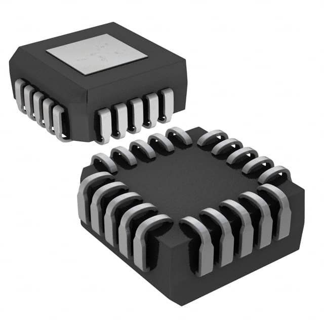
- Package: 20-pin plastic DIP (Dual In-line Package)
- Essence: Converts digital signals into analog voltages
- Packaging/Quantity: Tape and reel, 2500 units per reel
Specifications
- Resolution: 12 bits
- Supply Voltage: 2.7V to 5.5V
- Operating Temperature Range: -40°C to +85°C
- Output Voltage Range: 0V to Vref
- Reference Voltage Range: 2.5V to 5.5V
- Total Unadjusted Error: ±1 LSB (Least Significant Bit)
- Integral Nonlinearity: ±1 LSB
- Differential Nonlinearity: ±1 LSB
- Settling Time: 10µs
Detailed Pin Configuration
The MX7549JP+T has a total of 20 pins, which are assigned specific functions as follows:
- VDD: Positive supply voltage
- VREF: Reference voltage input
- AGND: Analog ground
- OUTA: Analog output A
- OUTB: Analog output B
- OUTC: Analog output C
- OUTD: Analog output D
- DGND: Digital ground
- DB0: Data bit 0
- DB1: Data bit 1
- DB2: Data bit 2
- DB3: Data bit 3
- DB4: Data bit 4
- DB5: Data bit 5
- DB6: Data bit 6
- DB7: Data bit 7
- WR: Write control input
- CS: Chip select input
- CLK: Clock input
- RESET: Reset input
Functional Features
- High-resolution DAC with 12-bit output
- Low power consumption for energy-efficient applications
- Wide operating voltage range allows for versatile use
- Fast settling time ensures accurate and responsive analog outputs
- Multiple analog output channels for increased flexibility
Advantages and Disadvantages
Advantages: - High precision and accuracy - Compact size for space-constrained designs - Low power consumption extends battery life - Versatile operating voltage range - Fast settling time for real-time applications
Disadvantages: - Limited number of analog output channels - Requires external reference voltage source - Sensitive to noise and interference in the environment
Working Principles
The MX7549JP+T is a digital-to-analog converter that converts digital signals into corresponding analog voltages. It utilizes a 12-bit resolution to provide high precision and accuracy in the conversion process. The IC operates by taking in digital data through the DB0-DB7 pins, which represent the binary input. The WR pin controls the write operation, while the CS pin selects the chip for communication. The CLK pin provides the necessary clock signal for synchronization.
Once the digital data is received, the MX7549JP+T internally processes it and generates the corresponding analog output voltages on the OUTA-OUTD pins. These analog outputs can be used to drive various analog devices or systems, such as audio amplifiers, motor control circuits, or sensor interfaces.
Detailed Application Field Plans
The MX7549JP+T finds applications in various fields where precise digital-to-analog conversion is required. Some potential application areas include:
- Audio Systems: The IC can be used in audio equipment to convert digital audio signals into analog voltages for amplification and playback.
- Industrial Automation: It can be utilized in industrial control systems to generate analog control signals for motor speed control, valve positioning, or temperature regulation.
- Instrumentation: The IC can be integrated into measurement instruments to convert digital sensor readings into analog outputs for display or further processing.
- Communication Systems: It can be employed in communication devices to convert digital signals into analog waveforms for transmission or modulation purposes.
Detailed and Complete Alternative Models
- MAX7549JP+T: Similar to MX7549JP+T, but manufactured by Maxim Integrated.
- LTC7549JP+T: Another alternative with similar specifications, produced by Linear Technology Corporation.
- AD7549JP+T: Analog Devices offers this alternative model, which provides comparable performance to the MX7549JP+T.
These alternative models offer similar functionality and characteristics, allowing users to choose the most suitable option based on their specific requirements.
Word count: 552 words
기술 솔루션에 MX7549JP+T 적용과 관련된 10가지 일반적인 질문과 답변을 나열하세요.
What is the operating temperature range of MX7549JP+T?
- The operating temperature range of MX7549JP+T is -40°C to 85°C.What is the typical input voltage for MX7549JP+T?
- The typical input voltage for MX7549JP+T is 5V.Can MX7549JP+T be used in automotive applications?
- Yes, MX7549JP+T is suitable for automotive applications.What is the maximum output current of MX7549JP+T?
- The maximum output current of MX7549JP+T is 20mA.Does MX7549JP+T require an external reference voltage?
- No, MX7549JP+T has a built-in reference voltage.Is MX7549JP+T RoHS compliant?
- Yes, MX7549JP+T is RoHS compliant.What is the package type of MX7549JP+T?
- MX7549JP+T is available in a 8-pin SOIC package.Can MX7549JP+T be used in battery-powered devices?
- Yes, MX7549JP+T can be used in battery-powered devices.What is the typical power consumption of MX7549JP+T?
- The typical power consumption of MX7549JP+T is 200μA.Is MX7549JP+T suitable for precision voltage measurement applications?
- Yes, MX7549JP+T is suitable for precision voltage measurement applications.