

ATF1504AS-15JC68
Product Overview
Category
ATF1504AS-15JC68 belongs to the category of programmable logic devices (PLDs).
Use
This product is commonly used in digital circuit design and implementation. It provides a flexible and customizable solution for various applications.
Characteristics
- Programmable: The ATF1504AS-15JC68 can be programmed to perform specific functions according to the user's requirements.
- High Integration: It integrates multiple logic gates, flip-flops, and other components into a single device, reducing the need for external components.
- Versatile: This PLD can be used in a wide range of applications, including telecommunications, automotive, industrial control, and consumer electronics.
Package
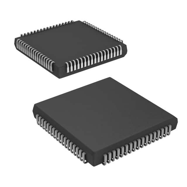
The ATF1504AS-15JC68 comes in a compact 68-pin PLCC (Plastic Leaded Chip Carrier) package.
Essence
The essence of ATF1504AS-15JC68 lies in its ability to provide reconfigurable logic functions, allowing designers to implement complex digital circuits efficiently.
Packaging/Quantity
This product is typically packaged in reels or tubes, with each containing a specific quantity of ATF1504AS-15JC68 units.
Specifications
- Operating Voltage: 3.3V
- Number of Logic Elements: 1504
- Maximum Frequency: 100 MHz
- Number of I/O Pins: 68
- Programmable Logic Blocks: 32
- On-Chip Memory: 8K bits
- JTAG Boundary Scan Support: Yes
Detailed Pin Configuration
The ATF1504AS-15JC68 has a total of 68 pins. Here is a detailed pin configuration:
- VCCIO1
- GND
- IO1_0
- IO1_1
- IO1_2
- IO1_3
- IO1_4
- IO1_5
- IO1_6
- IO1_7
- IO1_8
- IO1_9
- IO1_10
- IO1_11
- IO1_12
- IO1_13
- IO1_14
- IO1_15
- IO1_16
- IO1_17
- IO1_18
- IO1_19
- IO1_20
- IO1_21
- IO1_22
- IO1_23
- IO1_24
- IO1_25
- IO1_26
- IO1_27
- IO1_28
- IO1_29
- IO1_30
- IO1_31
- IO1_32
- IO1_33
- IO1_34
- IO1_35
- IO1_36
- IO1_37
- IO1_38
- IO1_39
- IO1_40
- IO1_41
- IO1_42
- IO1_43
- IO1_44
- IO1_45
- IO1_46
- IO1_47
- IO1_48
- IO1_49
- IO1_50
- IO1_51
- IO1_52
- IO1_53
- IO1_54
- IO1_55
- IO1_56
- IO1_57
- IO1_58
- IO1_59
- IO1_60
- IO1_61
- IO1_62
- IO1_63
- GND
- VCCIO2
Functional Features
- Reconfigurable Logic: The ATF1504AS-15JC68 allows users to program and reprogram the logic functions, enabling flexibility in circuit design.
- High-Speed Operation: With a maximum frequency of 100 MHz, this PLD can handle complex digital operations efficiently.
- JTAG Boundary Scan Support: The built-in JTAG boundary scan feature facilitates testing and debugging during development.
Advantages and Disadvantages
Advantages
- Flexibility: The ability to reconfigure the logic functions makes it suitable for various applications.
- Integration: The high integration level reduces the need for external components, saving space and cost.
- Versatility: It can be used in diverse industries due to its wide range of applications.
Disadvantages
- Learning Curve: Programming and utilizing the ATF1504AS-15JC68 may require some learning and expertise
기술 솔루션에 ATF1504AS-15JC68 적용과 관련된 10가지 일반적인 질문과 답변을 나열하세요.
Sure! Here are 10 common questions and answers related to the application of ATF1504AS-15JC68 in technical solutions:
Question: What is ATF1504AS-15JC68?
Answer: ATF1504AS-15JC68 is a specific model of Field Programmable Gate Array (FPGA) manufactured by Microchip Technology Inc.Question: What are the key features of ATF1504AS-15JC68?
Answer: Some key features of ATF1504AS-15JC68 include 1500 usable gates, 64 macrocells, 32 I/O pins, and a maximum operating frequency of 15 MHz.Question: In what applications can ATF1504AS-15JC68 be used?
Answer: ATF1504AS-15JC68 can be used in various applications such as industrial control systems, automotive electronics, telecommunications, and consumer electronics.Question: How can I program ATF1504AS-15JC68?
Answer: ATF1504AS-15JC68 can be programmed using industry-standard hardware description languages (HDLs) like VHDL or Verilog, along with appropriate development tools provided by the manufacturer.Question: Can ATF1504AS-15JC68 be reprogrammed after initial programming?
Answer: No, ATF1504AS-15JC68 is a one-time programmable (OTP) device, meaning it cannot be reprogrammed once it has been programmed.Question: What voltage levels does ATF1504AS-15JC68 support?
Answer: ATF1504AS-15JC68 supports both 3.3V and 5V voltage levels, making it compatible with a wide range of digital systems.Question: Does ATF1504AS-15JC68 have any built-in security features?
Answer: No, ATF1504AS-15JC68 does not have any built-in security features. Additional security measures need to be implemented at the system level if required.Question: Can ATF1504AS-15JC68 interface with other components or devices?
Answer: Yes, ATF1504AS-15JC68 can interface with other components or devices through its I/O pins, allowing for communication and integration within a larger system.Question: What is the power consumption of ATF1504AS-15JC68?
Answer: The power consumption of ATF1504AS-15JC68 depends on various factors such as the design complexity, operating frequency, and voltage levels used. It is recommended to refer to the datasheet for detailed power specifications.Question: Are there any specific design considerations when using ATF1504AS-15JC68?
Answer: Yes, some design considerations include proper decoupling of power supplies, managing signal integrity, and ensuring appropriate thermal management to prevent overheating during operation.
Please note that these answers are general in nature and may vary depending on the specific requirements and implementation of the technical solution.