

MCP3913A1-E/SS
Product Overview
Category
The MCP3913A1-E/SS belongs to the category of integrated circuits (ICs).
Use
This IC is commonly used in applications that require high-precision analog-to-digital conversion, such as power monitoring systems, energy measurement devices, and industrial instrumentation.
Characteristics
- High-resolution: The MCP3913A1-E/SS offers 24-bit delta-sigma ADCs for accurate data conversion.
- Low power consumption: It operates at low power levels, making it suitable for battery-powered devices.
- Wide input voltage range: The IC can handle a wide range of input voltages, allowing for versatile use in various applications.
- SPI interface: It features a Serial Peripheral Interface (SPI) for easy communication with microcontrollers or other digital devices.
- On-chip programmable gain amplifiers: The MCP3913A1-E/SS includes programmable gain amplifiers to enhance signal conditioning capabilities.
Package and Quantity
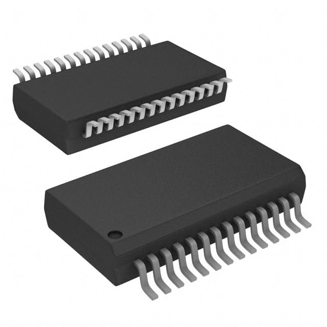
The MCP3913A1-E/SS is available in a small SSOP-28 package. It is typically sold in reels containing a specified quantity of ICs.
Specifications
- Resolution: 24 bits
- Input Voltage Range: -0.3V to VDD + 0.3V
- Supply Voltage: 2.7V to 5.5V
- Operating Temperature Range: -40°C to +125°C
- Sampling Rate: Up to 125 ksps (kilo samples per second)
- Number of ADC Channels: 2
Pin Configuration
The MCP3913A1-E/SS has a total of 28 pins. Here is a detailed pin configuration:
- VREFN: Negative reference voltage input
- VREFP: Positive reference voltage input
- AGND: Analog ground
- AVDD: Analog power supply
- DVDD: Digital power supply
- CLKOUT: Clock output
- MCLK: Master clock input
- RESET: Reset input
- CS: Chip select input
- SDO: Serial data output
- SDI: Serial data input
- SCK: Serial clock input
- DOUTA: ADC A data output
- DOUTB: ADC B data output
- VCM: Common-mode voltage output
- VINP0: Positive input channel 0
- VINN0: Negative input channel 0
- VINP1: Positive input channel 1
- VINN1: Negative input channel 1
- PGA0: Programmable gain amplifier control for channel 0
- PGA1: Programmable gain amplifier control for channel 1
- REFOUT: Reference voltage output
- REFIN: Reference voltage input
- CLKIN: External clock input
- NC: No connection
- NC: No connection
- NC: No connection
- NC: No connection
Functional Features
- High-resolution ADCs: The MCP3913A1-E/SS provides two 24-bit delta-sigma ADCs, enabling precise analog-to-digital conversion.
- Programmable Gain Amplifiers (PGAs): Integrated PGAs allow users to adjust the gain of the input signals, enhancing flexibility in signal conditioning.
- SPI Interface: The IC utilizes an SPI interface for easy integration with microcontrollers or other digital devices.
- Low Power Consumption: The MCP3913A1-E/SS operates at low power levels, making it suitable for energy-efficient applications.
- Reference Voltage Output: It offers a reference voltage output for external use, simplifying system design.
Advantages and Disadvantages
Advantages
- High-resolution ADCs ensure accurate data conversion.
- Programmable gain amplifiers provide flexibility in signal conditioning.
- Low power consumption extends battery life in portable applications.
- Wide input voltage range allows for versatile use.
- SPI interface enables easy communication with digital devices.
Disadvantages
- Limited number of ADC channels (2) may not be sufficient for certain applications requiring more inputs.
- The SSOP-28 package may pose challenges for manual soldering or prototyping.
Working Principles
The MCP3913A1-E/SS utilizes delta-sigma modulation techniques to convert analog signals into digital data. It employs a combination of oversampling and noise shaping to achieve high resolution and accuracy. The programmable gain amplifiers help amplify and condition the input signals before conversion. The IC communicates with external devices through the SPI interface, allowing for seamless integration into various systems.
Detailed Application Field Plans
The MCP3913A1-E/SS finds application in various fields, including: - Power monitoring systems: It accurately measures power consumption and provides valuable data for energy management. - Energy measurement devices: The IC enables
기술 솔루션에 MCP3913A1-E/SS 적용과 관련된 10가지 일반적인 질문과 답변을 나열하세요.
What is the maximum sampling rate of MCP3913A1-E/SS?
- The maximum sampling rate of MCP3913A1-E/SS is 125 kSPS.Can MCP3913A1-E/SS be used in single-phase energy metering applications?
- Yes, MCP3913A1-E/SS can be used in single-phase energy metering applications.What is the operating voltage range of MCP3913A1-E/SS?
- The operating voltage range of MCP3913A1-E/SS is 2.7V to 5.5V.Does MCP3913A1-E/SS support SPI communication?
- Yes, MCP3913A1-E/SS supports SPI communication.Is MCP3913A1-E/SS suitable for power monitoring and control systems?
- Yes, MCP3913A1-E/SS is suitable for power monitoring and control systems.What is the resolution of the ADC in MCP3913A1-E/SS?
- The ADC in MCP3913A1-E/SS has a resolution of 24 bits.Can MCP3913A1-E/SS be used in industrial automation applications?
- Yes, MCP3913A1-E/SS can be used in industrial automation applications.What is the typical power consumption of MCP3913A1-E/SS?
- The typical power consumption of MCP3913A1-E/SS is 7.5 mW.Does MCP3913A1-E/SS have built-in programmable gain amplifiers (PGAs)?
- Yes, MCP3913A1-E/SS has built-in PGAs with gains of 1, 2, 4, and 8.Is MCP3913A1-E/SS RoHS compliant?
- Yes, MCP3913A1-E/SS is RoHS compliant.