

MIC2583-MYQS-TR
Product Overview
Category
MIC2583-MYQS-TR belongs to the category of integrated circuits (ICs) specifically designed for power management applications.
Use
This product is primarily used for controlling and managing power in various electronic devices and systems.
Characteristics
- High efficiency power management
- Compact size
- Low power consumption
- Wide input voltage range
- Overcurrent protection
- Thermal shutdown protection
Package
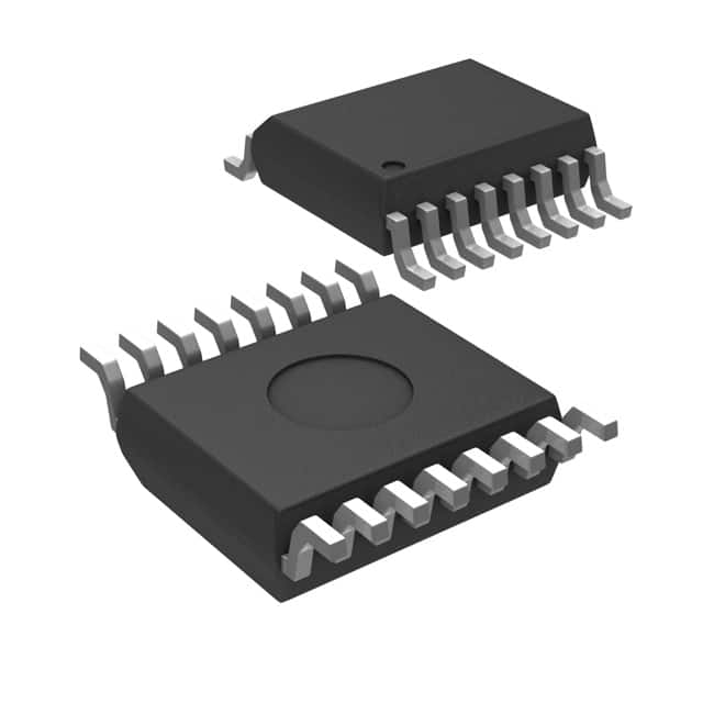
MIC2583-MYQS-TR is available in a small outline package (SOP) with a specific pin configuration.
Essence
The essence of this product lies in its ability to efficiently regulate and control power flow within electronic devices, ensuring optimal performance and protection against potential damage.
Packaging/Quantity
MIC2583-MYQS-TR is typically packaged in reels or tubes, with each reel/tube containing a specific quantity of ICs. The exact packaging and quantity may vary depending on the manufacturer.
Specifications
- Input Voltage Range: 4.5V - 40V
- Output Voltage Range: 0.8V - 37V
- Maximum Output Current: 3A
- Operating Temperature Range: -40°C to +125°C
- Package Type: SOP-8
Detailed Pin Configuration
- VIN: Input voltage pin
- GND: Ground pin
- EN: Enable pin
- FB: Feedback pin
- COMP: Compensation pin
- SS/TR: Soft-start/Tracking pin
- PGND: Power ground pin
- VOUT: Output voltage pin
Functional Features
- Wide input voltage range allows compatibility with various power sources.
- Efficient power management ensures minimal energy loss.
- Overcurrent protection safeguards the device and connected components.
- Thermal shutdown protection prevents overheating and damage.
- Soft-start feature enables smooth power-up, reducing stress on the system.
Advantages and Disadvantages
Advantages
- High efficiency power management leads to energy savings.
- Compact size allows for integration into space-constrained designs.
- Wide input voltage range provides flexibility in power source selection.
- Overcurrent and thermal protection enhance device reliability.
Disadvantages
- Limited maximum output current may not be suitable for high-power applications.
- SOP package may require additional heat dissipation measures in certain scenarios.
Working Principles
MIC2583-MYQS-TR operates based on a switching regulator topology. It utilizes a combination of control circuitry, power MOSFETs, and feedback mechanisms to regulate the input voltage and provide a stable output voltage. The integrated protection features ensure safe operation under various conditions.
Detailed Application Field Plans
MIC2583-MYQS-TR finds applications in a wide range of electronic devices and systems, including but not limited to: - Power supplies - Battery chargers - LED lighting systems - Industrial automation equipment - Automotive electronics
Detailed and Complete Alternative Models
- MIC2584-MYQS-TR: Similar specifications and features, with an extended maximum output current of 5A.
- LT8610-1: Higher efficiency and wider input voltage range, suitable for demanding power management applications.
- TPS54332: Integrated synchronous buck converter with adjustable output voltage and higher maximum output current.
These alternative models offer similar functionality and can be considered as alternatives to MIC2583-MYQS-TR depending on specific requirements and design constraints.
Word count: 520 words
기술 솔루션에 MIC2583-MYQS-TR 적용과 관련된 10가지 일반적인 질문과 답변을 나열하세요.
Sure! Here are 10 common questions and answers related to the application of MIC2583-MYQS-TR in technical solutions:
Q: What is MIC2583-MYQS-TR? A: MIC2583-MYQS-TR is a high-performance, dual-channel MOSFET driver IC designed for driving N-channel enhancement-mode MOSFETs in various applications.
Q: What is the maximum operating voltage of MIC2583-MYQS-TR? A: The maximum operating voltage of MIC2583-MYQS-TR is typically 18V.
Q: Can MIC2583-MYQS-TR be used in automotive applications? A: Yes, MIC2583-MYQS-TR is suitable for automotive applications as it meets the necessary requirements for automotive-grade components.
Q: What is the maximum output current capability of each channel in MIC2583-MYQS-TR? A: Each channel of MIC2583-MYQS-TR can provide a maximum output current of up to 2A.
Q: Is MIC2583-MYQS-TR compatible with both TTL and CMOS logic levels? A: Yes, MIC2583-MYQS-TR is compatible with both TTL (Transistor-Transistor Logic) and CMOS (Complementary Metal-Oxide-Semiconductor) logic levels.
Q: Can MIC2583-MYQS-TR handle PWM (Pulse Width Modulation) signals? A: Yes, MIC2583-MYQS-TR can handle PWM signals and is commonly used in applications that require precise control of power delivery.
Q: Does MIC2583-MYQS-TR have built-in protection features? A: Yes, MIC2583-MYQS-TR incorporates various protection features such as thermal shutdown, under-voltage lockout, and shoot-through protection.
Q: What is the typical propagation delay of MIC2583-MYQS-TR? A: The typical propagation delay of MIC2583-MYQS-TR is around 30ns, which ensures fast switching performance.
Q: Can MIC2583-MYQS-TR be used in high-frequency applications? A: Yes, MIC2583-MYQS-TR is suitable for high-frequency applications as it has a wide bandwidth and low output impedance.
Q: Are there any application notes or reference designs available for MIC2583-MYQS-TR? A: Yes, the manufacturer provides application notes and reference designs that can help users understand and implement MIC2583-MYQS-TR in their specific technical solutions.
Please note that the answers provided here are general and may vary depending on the specific requirements and conditions of each application.