

PIC18LF24J50-I/SO
Product Overview
- Category: Microcontroller
- Use: Embedded systems, Internet of Things (IoT) devices, consumer electronics
- Characteristics: Low power consumption, high performance, versatile functionality
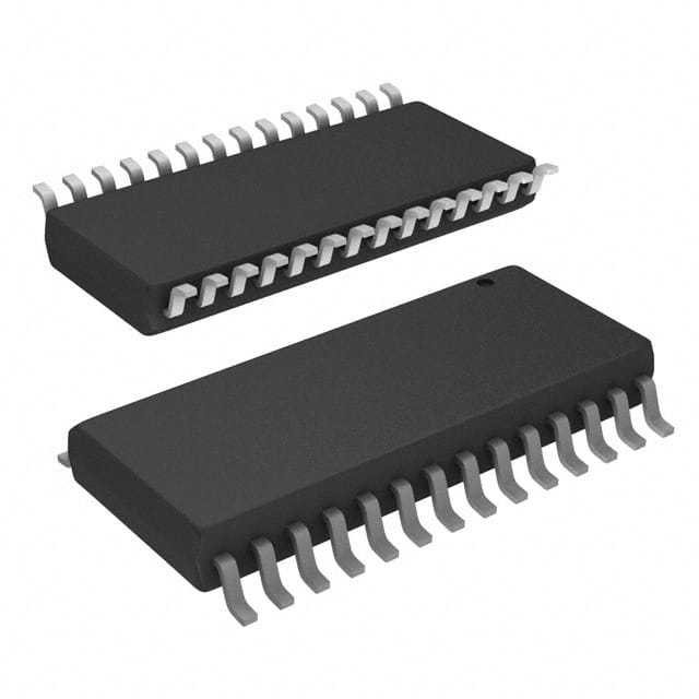
- Package: SOIC (Small Outline Integrated Circuit)
- Essence: A powerful microcontroller designed for various applications requiring low power and high performance.
- Packaging/Quantity: Available in tape and reel packaging, with a quantity of 250 units per reel.
Specifications
- Architecture: 8-bit
- Flash Memory: 24KB
- RAM: 2KB
- Operating Voltage: 2.3V to 5.5V
- Operating Temperature Range: -40°C to +85°C
- Number of I/O Pins: 20
- Communication Interfaces: SPI, I2C, UART
- Analog-to-Digital Converter (ADC): 10-bit, 13 channels
- Timers: 4 x 8-bit, 1 x 16-bit
- PWM Channels: 5
- Clock Speed: Up to 48 MHz
Detailed Pin Configuration
The PIC18LF24J50-I/SO microcontroller has a total of 20 pins, which are assigned for various functions such as I/O, power supply, communication, and programming. The pin configuration is as follows:
- VDD - Power Supply
- RA0/AN0 - Analog Input/Output or Digital I/O
- RA1/AN1 - Analog Input/Output or Digital I/O
- RA2/AN2 - Analog Input/Output or Digital I/O
- RA3/AN3/VREF-/CVREF - Analog Input/Output or Digital I/O
- RA4/T0CKI/C1OUT - Timer0 Clock Input or Digital I/O
- VSS - Ground
- RA5/AN4/SS/HLVDIN - Analog Input/Output, Slave Select or High/Low Voltage Detect Input
- RE0/INT0/FLTA/CCP2 - External Interrupt 0, Fault Input A or Capture/Compare/PWM 2
- RE1/INT1/FLTB/CCP3 - External Interrupt 1, Fault Input B or Capture/Compare/PWM 3
- RE2/INT2/VMO/CCP4 - External Interrupt 2, Voltage Monitor Output or Capture/Compare/PWM 4
- VUSB - USB Power Supply
- RB0/PGM/CCP1 - Programming/Data Memory Interface or Capture/Compare/PWM 1
- RB1/PGC/CCP5 - Programming/Debug Clock or Capture/Compare/PWM 5
- RB2/PGD - Programming/Debug Data
- RB3/SCL/SCK - I2C Serial Clock or SPI Serial Clock
- RB4/SDA/SDI - I2C Serial Data or SPI Serial Data Input
- RB5/SDO - SPI Serial Data Output
- RB6/PGM - Programming/Data Memory Interface
- RB7/PGC - Programming/Debug Clock
Functional Features
- Low power consumption: The PIC18LF24J50-I/SO microcontroller is designed to operate efficiently with low power requirements, making it suitable for battery-powered devices.
- High performance: With a clock speed of up to 48 MHz and a powerful 8-bit architecture, this microcontroller offers fast and reliable processing capabilities.
- Versatile functionality: It supports various communication interfaces such as SPI, I2C, and UART, enabling seamless integration with other devices.
- Analog-to-Digital Converter (ADC): The built-in 10-bit ADC allows for accurate analog signal measurements and conversions.
- Timers and PWM Channels: Multiple timers and PWM channels provide precise timing control and enable the generation of analog-like signals.
Advantages and Disadvantages
Advantages
- Low power consumption extends battery life in portable applications.
- Versatile functionality allows for flexible system design and integration.
- High-performance processing capabilities enable efficient execution of complex tasks.
- Built-in ADC simplifies analog signal processing.
- Ample I/O pins provide flexibility for connecting external devices.
Disadvantages
- Limited flash memory capacity may restrict the size of the firmware or program that can be stored.
- The 8-bit architecture may not be suitable for applications requiring extensive computational power.
- Lack of built-in Ethernet or Wi-Fi connectivity may require additional components for networking capabilities.
Working Principles
The PIC18LF24J50-I/SO microcontroller operates based on the Harvard architecture, which separates program memory and data memory. It executes
기술 솔루션에 PIC18LF24J50-I/SO 적용과 관련된 10가지 일반적인 질문과 답변을 나열하세요.
What is the maximum operating frequency of PIC18LF24J50-I/SO?
- The maximum operating frequency of PIC18LF24J50-I/SO is 32 MHz.Can PIC18LF24J50-I/SO be used in battery-powered applications?
- Yes, PIC18LF24J50-I/SO is suitable for battery-powered applications due to its low power consumption.What are the communication interfaces supported by PIC18LF24J50-I/SO?
- PIC18LF24J50-I/SO supports SPI, I2C, and UART communication interfaces.Is PIC18LF24J50-I/SO compatible with 5V systems?
- No, PIC18LF24J50-I/SO operates at a maximum voltage of 3.6V and is not directly compatible with 5V systems.Can PIC18LF24J50-I/SO be used for USB connectivity?
- Yes, PIC18LF24J50-I/SO features USB 2.0 support for connectivity.What development tools are available for programming PIC18LF24J50-I/SO?
- Development tools such as MPLAB X IDE and PICkit programmers can be used for programming PIC18LF24J50-I/SO.Does PIC18LF24J50-I/SO have built-in analog-to-digital converters (ADC)?
- Yes, PIC18LF24J50-I/SO has integrated 10-bit ADC modules.What is the flash memory size of PIC18LF24J50-I/SO?
- PIC18LF24J50-I/SO has 16 KB of flash memory for program storage.Can PIC18LF24J50-I/SO be used in industrial control applications?
- Yes, PIC18LF24J50-I/SO is suitable for industrial control applications due to its robust features and peripherals.Are there any application notes or reference designs available for PIC18LF24J50-I/SO?
- Yes, Microchip provides application notes and reference designs for implementing PIC18LF24J50-I/SO in various technical solutions.