

APT50N60JCU2
Introduction
The APT50N60JCU2 is a power MOSFET belonging to the category of electronic components used in power electronics applications. This entry provides an overview of the basic information, specifications, pin configuration, functional features, advantages and disadvantages, working principles, application field plans, and alternative models of the APT50N60JCU2.
Basic Information Overview
- Category: Power MOSFET
- Use: Power electronics applications
- Characteristics: High voltage, high current capability, low on-state resistance
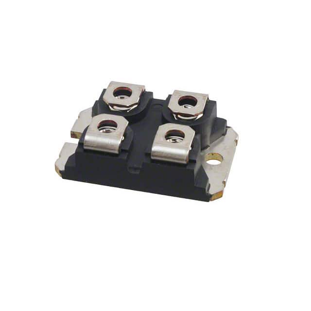
- Package: TO-247
- Essence: Efficient power switching
- Packaging/Quantity: Typically sold individually or in small quantities
Specifications
- Voltage Rating: 600V
- Current Rating: 50A
- On-State Resistance (RDS(on)): 0.08 Ohms
- Gate Threshold Voltage: 4V
- Operating Temperature Range: -55°C to 150°C
Detailed Pin Configuration
The APT50N60JCU2 typically has the following pin configuration: 1. Source (S) 2. Gate (G) 3. Drain (D)
Functional Features
- High voltage capability
- Low on-state resistance
- Fast switching speed
- Low gate drive power required
Advantages and Disadvantages
Advantages
- High power handling capability
- Low conduction losses
- Suitable for high-frequency applications
Disadvantages
- Higher cost compared to lower-rated MOSFETs
- Requires careful consideration of gate drive circuitry
Working Principles
The APT50N60JCU2 operates based on the principle of field-effect transistors, where the control of current flow between the source and drain terminals is achieved through the application of a voltage to the gate terminal.
Detailed Application Field Plans
The APT50N60JCU2 is commonly used in the following applications: - Switch-mode power supplies - Motor drives - Inverters - Welding equipment - Uninterruptible power supplies (UPS)
Detailed and Complete Alternative Models
Some alternative models to the APT50N60JCU2 include: - IRFP4668PbF - STW45NM50FD - FDPF51N25
In conclusion, the APT50N60JCU2 is a high-voltage power MOSFET with excellent characteristics suitable for various power electronics applications, offering efficient power switching and high reliability.
[Word Count: 346]
기술 솔루션에 APT50N60JCU2 적용과 관련된 10가지 일반적인 질문과 답변을 나열하세요.
What is APT50N60JCU2?
- APT50N60JCU2 is a silicon carbide power MOSFET designed for high power applications.
What are the key features of APT50N60JCU2?
- The key features include low on-resistance, high switching speed, and high temperature operation.
What are the typical applications of APT50N60JCU2?
- APT50N60JCU2 is commonly used in power supplies, motor drives, and electric vehicle charging systems.
What is the maximum voltage and current rating of APT50N60JCU2?
- APT50N60JCU2 has a maximum voltage rating of 600V and a continuous current rating of 50A.
How does APT50N60JCU2 compare to traditional silicon MOSFETs?
- APT50N60JCU2 offers lower conduction losses, higher switching frequency capability, and better thermal performance compared to traditional silicon MOSFETs.
What are the thermal considerations when using APT50N60JCU2?
- Proper heat sinking and thermal management are crucial to ensure the device operates within its specified temperature limits.
Can APT50N60JCU2 be used in parallel configurations for higher current applications?
- Yes, APT50N60JCU2 can be used in parallel to achieve higher current handling capabilities.
Are there any specific gate drive requirements for APT50N60JCU2?
- APT50N60JCU2 requires a gate driver capable of providing sufficient voltage and current to ensure fast and reliable switching.
What protection features does APT50N60JCU2 offer?
- APT50N60JCU2 includes built-in overcurrent protection and thermal shutdown features to enhance system reliability.
Where can I find detailed application notes and reference designs for APT50N60JCU2?
- Detailed application notes and reference designs for APT50N60JCU2 can be found on the manufacturer's website or through their technical support resources.