

LX7175CLD-TR
Product Overview
Category
LX7175CLD-TR belongs to the category of integrated circuits (ICs).
Use
This product is commonly used in electronic devices for voltage regulation and power management.
Characteristics
The LX7175CLD-TR is known for its high efficiency, low dropout voltage, and excellent line and load regulation capabilities. It is designed to provide stable and reliable power supply solutions.
Package
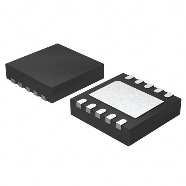
The LX7175CLD-TR comes in a small outline package (SOP) with a thermal pad for efficient heat dissipation.
Essence
The essence of LX7175CLD-TR lies in its ability to regulate voltage effectively, ensuring consistent and reliable power supply to electronic devices.
Packaging/Quantity
The LX7175CLD-TR is typically packaged in reels, with each reel containing a specific quantity of ICs. The exact quantity may vary depending on the manufacturer's specifications.
Specifications
The following are the detailed specifications of LX7175CLD-TR:
- Input Voltage Range: 2.7V to 5.5V
- Output Voltage Range: 1.2V to 3.6V
- Maximum Output Current: 500mA
- Dropout Voltage: 200mV at 500mA
- Line Regulation: ±0.05% typical
- Load Regulation: ±0.1% typical
- Quiescent Current: 75µA typical
- Operating Temperature Range: -40°C to +85°C
Pin Configuration
The LX7175CLD-TR has the following pin configuration:
- VIN (Input Voltage)
- GND (Ground)
- EN (Enable)
- FB (Feedback)
- VOUT (Output Voltage)
Functional Features
The LX7175CLD-TR offers the following functional features:
- Low dropout voltage for efficient power conversion
- Excellent line and load regulation for stable output voltage
- Thermal shutdown protection to prevent overheating
- Enable pin for easy on/off control
- Short-circuit current limit for enhanced safety
Advantages and Disadvantages
Advantages
- High efficiency power management solution
- Wide input voltage range for versatile applications
- Compact package with thermal pad for effective heat dissipation
- Low quiescent current for power-saving operation
Disadvantages
- Limited maximum output current of 500mA
- Dropout voltage of 200mV may not be suitable for ultra-low power devices
Working Principles
The LX7175CLD-TR operates based on a linear regulator architecture. It regulates the output voltage by adjusting the resistance between the input and output terminals, ensuring a stable voltage despite variations in the input voltage or load conditions.
Detailed Application Field Plans
The LX7175CLD-TR finds applications in various electronic devices that require voltage regulation and power management. Some potential application fields include:
- Mobile devices: Smartphones, tablets, and portable media players.
- Wireless communication systems: Bluetooth headsets, Wi-Fi modules, and IoT devices.
- Consumer electronics: Digital cameras, portable gaming consoles, and MP3 players.
- Industrial equipment: Data loggers, measurement instruments, and control systems.
- Automotive electronics: Infotainment systems, GPS devices, and dashboard displays.
Detailed and Complete Alternative Models
Some alternative models that offer similar functionality to LX7175CLD-TR are:
- LM1117-3.3: A popular linear regulator with a fixed output voltage of 3.3V.
- LT1763: A low dropout linear regulator with adjustable output voltage.
- TPS7A47: An ultra-low noise linear regulator suitable for sensitive applications.
- ADP3339: A high-current linear regulator with a wide input voltage range.
These alternative models can be considered based on specific requirements and design constraints.
Word count: 511 words
기술 솔루션에 LX7175CLD-TR 적용과 관련된 10가지 일반적인 질문과 답변을 나열하세요.
Sure! Here are 10 common questions and answers related to the application of LX7175CLD-TR in technical solutions:
Q: What is LX7175CLD-TR? A: LX7175CLD-TR is a voltage regulator IC (integrated circuit) that provides a stable output voltage for various electronic devices.
Q: What is the input voltage range for LX7175CLD-TR? A: The input voltage range for LX7175CLD-TR is typically between 2.7V and 5.5V.
Q: What is the output voltage range of LX7175CLD-TR? A: The output voltage range of LX7175CLD-TR can be adjusted from 0.8V to 3.6V using external resistors.
Q: What is the maximum output current of LX7175CLD-TR? A: The maximum output current of LX7175CLD-TR is typically 500mA.
Q: Can LX7175CLD-TR be used in battery-powered applications? A: Yes, LX7175CLD-TR can be used in battery-powered applications as it operates within a wide input voltage range and has low quiescent current.
Q: Does LX7175CLD-TR have built-in thermal protection? A: Yes, LX7175CLD-TR has built-in thermal shutdown protection to prevent overheating and damage.
Q: Can LX7175CLD-TR be used in automotive applications? A: Yes, LX7175CLD-TR is suitable for automotive applications as it meets the necessary requirements for temperature, voltage, and reliability.
Q: Is LX7175CLD-TR compatible with both analog and digital circuits? A: Yes, LX7175CLD-TR can be used with both analog and digital circuits as it provides a stable output voltage for various electronic devices.
Q: Can LX7175CLD-TR be used in low-power applications? A: Yes, LX7175CLD-TR is suitable for low-power applications as it has low quiescent current and high efficiency.
Q: Are there any application notes or reference designs available for LX7175CLD-TR? A: Yes, the manufacturer of LX7175CLD-TR provides application notes and reference designs that can help in implementing the IC in different technical solutions.
Please note that the answers provided here are general and may vary depending on specific requirements and use cases. It's always recommended to refer to the datasheet and consult with the manufacturer for detailed information and application-specific guidance.