

74AHCT1G125GV,125
Basic Information Overview
- Category: Integrated Circuit (IC)
- Use: Buffer/Driver
- Characteristics: High-speed, low-power, single-gate buffer/driver
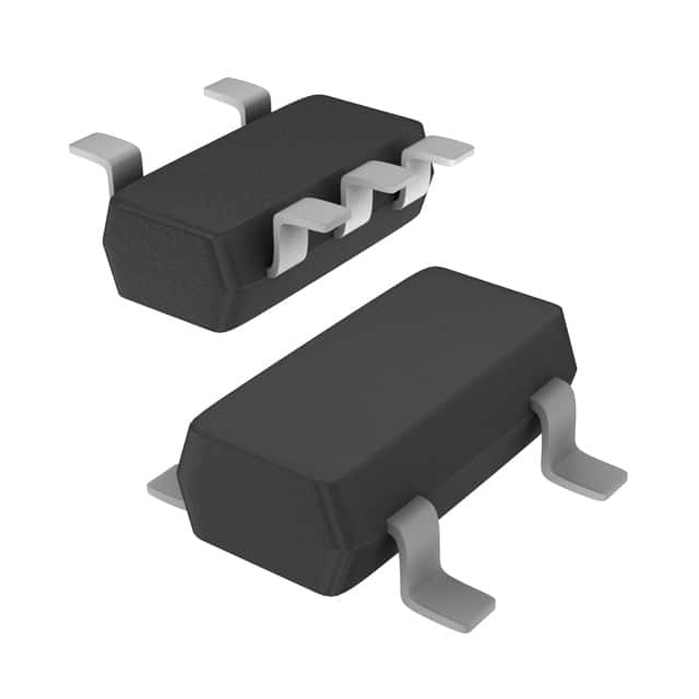
- Package: SOT753 (SC-70)
- Essence: Single gate non-inverting buffer/driver
- Packaging/Quantity: Tape and Reel, 3000 pieces per reel
Specifications
- Supply Voltage Range: 4.5V to 5.5V
- Input Voltage Range: 0V to VCC
- Output Voltage Range: 0V to VCC
- Maximum Operating Frequency: 400 MHz
- Output Current: ±8 mA
- Propagation Delay: 3.5 ns (typical)
- Input Capacitance: 3 pF (typical)
- Operating Temperature Range: -40°C to +85°C
Detailed Pin Configuration
The 74AHCT1G125GV,125 IC has a total of 5 pins: 1. Pin 1: GND (Ground) 2. Pin 2: A (Input) 3. Pin 3: Y (Output) 4. Pin 4: NC (No Connection) 5. Pin 5: VCC (Power Supply)
Functional Features
- Non-inverting buffer/driver with high-speed performance
- Compatible with TTL and CMOS logic levels
- Provides buffering and driving capabilities for digital signals
- Low power consumption
- Wide operating voltage range
- Schmitt-trigger input for improved noise immunity
Advantages and Disadvantages
Advantages: - High-speed operation allows for efficient signal transmission - Low power consumption helps in reducing overall system power requirements - Compatibility with both TTL and CMOS logic levels enables versatile usage - Schmitt-trigger input enhances noise immunity, ensuring reliable signal processing
Disadvantages: - Limited output current may restrict usage in certain applications requiring higher drive capabilities - Single gate configuration limits the number of signals that can be buffered/driven simultaneously
Working Principles
The 74AHCT1G125GV,125 is a single-gate buffer/driver IC. It takes an input signal (A) and provides a non-inverted output signal (Y). The IC operates as a voltage amplifier, boosting the input signal to a level suitable for driving other digital components. It is designed to operate at high speeds while consuming minimal power.
Detailed Application Field Plans
The 74AHCT1G125GV,125 finds applications in various fields, including but not limited to: 1. Digital communication systems 2. Computer peripherals 3. Industrial automation 4. Consumer electronics 5. Automotive electronics
Detailed and Complete Alternative Models
Some alternative models that offer similar functionality to the 74AHCT1G125GV,125 are: 1. SN74LVC1G125DBVR - Texas Instruments 2. NC7SZ125P5X - ON Semiconductor 3. MC74VHC1GT125DF1G - ON Semiconductor 4. TC7SZ125FU - Toshiba 5. 74LVC1G125GW - NXP Semiconductors
(Note: The above list is not exhaustive and serves as a reference for alternative options.)
This entry provides an overview of the 74AHCT1G125GV,125 IC, including its basic information, specifications, pin configuration, functional features, advantages, disadvantages, working principles, application field plans, and alternative models.
기술 솔루션에 74AHCT1G125GV,125 적용과 관련된 10가지 일반적인 질문과 답변을 나열하세요.
Sure! Here are 10 common questions and answers related to the application of 74AHCT1G125GV,125 in technical solutions:
Q1: What is the function of the 74AHCT1G125GV,125? A1: The 74AHCT1G125GV,125 is a single bus buffer gate with 3-state output. It is used to control the flow of data between different parts of a circuit.
Q2: What is the voltage range supported by the 74AHCT1G125GV,125? A2: The 74AHCT1G125GV,125 supports a voltage range of 4.5V to 5.5V.
Q3: How many inputs does the 74AHCT1G125GV,125 have? A3: The 74AHCT1G125GV,125 has one input.
Q4: How many outputs does the 74AHCT1G125GV,125 have? A4: The 74AHCT1G125GV,125 has one output.
Q5: What is the maximum output current of the 74AHCT1G125GV,125? A5: The maximum output current of the 74AHCT1G125GV,125 is 8mA.
Q6: Can the 74AHCT1G125GV,125 be used for level shifting? A6: Yes, the 74AHCT1G125GV,125 can be used for level shifting as it supports both TTL and CMOS logic levels.
Q7: Is the 74AHCT1G125GV,125 compatible with other logic families? A7: Yes, the 74AHCT1G125GV,125 is compatible with other logic families such as LVTTL, LVCMOS, and HSTL.
Q8: What is the propagation delay of the 74AHCT1G125GV,125? A8: The propagation delay of the 74AHCT1G125GV,125 is typically around 5ns.
Q9: Can the 74AHCT1G125GV,125 be used in high-speed applications? A9: Yes, the 74AHCT1G125GV,125 can be used in high-speed applications as it has a maximum frequency rating of 200MHz.
Q10: Is the 74AHCT1G125GV,125 available in different package options? A10: Yes, the 74AHCT1G125GV,125 is available in different package options such as SOT23 and SC-70.
Please note that the answers provided here are general and may vary depending on specific datasheet specifications or application requirements.