

Encyclopedia Entry: 74ALVCH16374DL,112
Product Overview
Category
The 74ALVCH16374DL,112 belongs to the category of integrated circuits (ICs) and specifically falls under the family of flip-flops.
Use
This product is commonly used in digital electronic systems for data storage and transfer. It serves as a D-type flip-flop with 16-bit wide output registers.
Characteristics
- High-speed operation
- Low power consumption
- Wide operating voltage range
- Schmitt-trigger action on all inputs
- Balanced propagation delays
- Symmetrical output impedance
Package
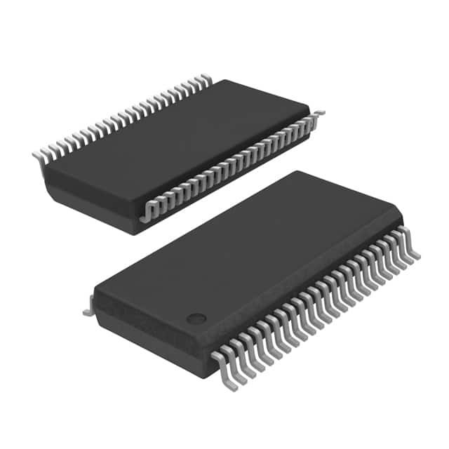
The 74ALVCH16374DL,112 is available in a small-outline package (SO) with 48 pins.
Essence
The essence of this product lies in its ability to store and transfer digital data efficiently within electronic systems.
Packaging/Quantity
The 74ALVCH16374DL,112 is typically packaged in reels or tubes, containing a quantity of 250 units per package.
Specifications
- Supply Voltage Range: 1.2V to 3.6V
- Input Voltage Range: -0.5V to VCC + 0.5V
- Output Voltage Range: 0V to VCC
- Operating Temperature Range: -40°C to +85°C
- Input Capacitance: 4pF
- Output Capacitance: 8pF
- Propagation Delay: 2.5ns (max)
- Output Current: ±24mA
Detailed Pin Configuration
The 74ALVCH16374DL,112 has a total of 48 pins, which are assigned specific functions. The pin configuration is as follows:
- Pin 1: Data Input (D0)
- Pin 2: Data Input (D1)
- Pin 3: Data Input (D2)
- Pin 4: Data Input (D3)
- Pin 5: Data Input (D4)
- Pin 6: Data Input (D5)
- Pin 7: Data Input (D6)
- Pin 8: Data Input (D7)
- Pin 9: Data Input (D8)
- Pin 10: Data Input (D9)
- Pin 11: Data Input (D10)
- Pin 12: Data Input (D11)
- Pin 13: Data Input (D12)
- Pin 14: Data Input (D13)
- Pin 15: Data Input (D14)
- Pin 16: Data Input (D15)
- Pin 17: Clock Input (CP)
- Pin 18: Output Enable (OE)
- Pin 19: Master Reset (MR)
- Pin 20: GND (Ground)
- Pin 21: Output Q0
- Pin 22: Output Q1
- Pin 23: Output Q2
- Pin 24: Output Q3
- Pin 25: Output Q4
- Pin 26: Output Q5
- Pin 27: Output Q6
- Pin 28: Output Q7
- Pin 29: Output Q8
- Pin 30: Output Q9
- Pin 31: Output Q10
- Pin 32: Output Q11
- Pin 33: Output Q12
- Pin 34: Output Q13
- Pin 35: Output Q14
- Pin 36: Output Q15
- Pin 37: VCC (Supply Voltage)
Functional Features
The 74ALVCH16374DL,112 offers the following functional features:
- Data Storage: The flip-flop design allows for the storage of digital data on the inputs.
- Data Transfer: The stored data can be transferred to the output registers upon receiving a clock signal.
- Output Enable: The output enable pin allows for controlling the output state.
- Master Reset: The master reset pin resets all outputs to a predefined state.
Advantages and Disadvantages
Advantages
- High-speed operation enables efficient data transfer.
- Low power consumption contributes to energy efficiency.
- Wide operating voltage range provides flexibility in various electronic systems.
- Schmitt-trigger action on all inputs ensures reliable signal processing.
- Balanced propagation delays enhance overall system performance.
- Symmetrical output impedance simplifies circuit design.
Disadvantages
- Limited number of output registers (16-bit) may not suffice for certain applications requiring larger data storage.
- Availability in a specific package (SO) may limit compatibility with certain circuit designs.
Working Principles
The 74ALVCH16374DL,112
기술 솔루션에 74ALVCH16374DL,112 적용과 관련된 10가지 일반적인 질문과 답변을 나열하세요.
Sure! Here are 10 common questions and answers related to the application of 74ALVCH16374DL,112 in technical solutions:
Q: What is the function of the 74ALVCH16374DL,112? A: The 74ALVCH16374DL,112 is a 16-bit D-type flip-flop with 3-state outputs. It can store and transfer data in digital circuits.
Q: What is the operating voltage range for this IC? A: The 74ALVCH16374DL,112 operates within a voltage range of 1.65V to 3.6V.
Q: How many flip-flops are there in the 74ALVCH16374DL,112? A: The 74ALVCH16374DL,112 contains 16 individual D-type flip-flops.
Q: What is the maximum clock frequency supported by this IC? A: The 74ALVCH16374DL,112 can operate at a maximum clock frequency of 400MHz.
Q: Can I use this IC in both synchronous and asynchronous applications? A: Yes, the 74ALVCH16374DL,112 can be used in both synchronous and asynchronous applications.
Q: What is the output drive strength of this IC? A: The 74ALVCH16374DL,112 has a typical output drive strength of ±24mA.
Q: Does this IC have any power-saving features? A: Yes, the 74ALVCH16374DL,112 has a power-down mode that reduces power consumption when not in use.
Q: Can I cascade multiple 74ALVCH16374DL,112 ICs together? A: Yes, you can cascade multiple 74ALVCH16374DL,112 ICs to increase the number of flip-flops in your circuit.
Q: What is the typical propagation delay of this IC? A: The typical propagation delay for the 74ALVCH16374DL,112 is around 2.5ns.
Q: Are there any special considerations when designing with this IC? A: It is important to ensure proper decoupling and power supply bypassing to minimize noise and voltage fluctuations in the circuit. Additionally, attention should be given to signal integrity and timing requirements.
Please note that the answers provided here are general and may vary depending on specific datasheet specifications and application requirements.