

Encyclopedia Entry: 74ALVT162821DL,518
Product Overview
Category
The 74ALVT162821DL,518 belongs to the category of integrated circuits (ICs).
Use
This IC is commonly used in digital electronic systems for data storage and manipulation.
Characteristics
- High-speed operation
- Low power consumption
- Wide operating voltage range
- Compatibility with various logic families
- Robustness against noise and interference
Package
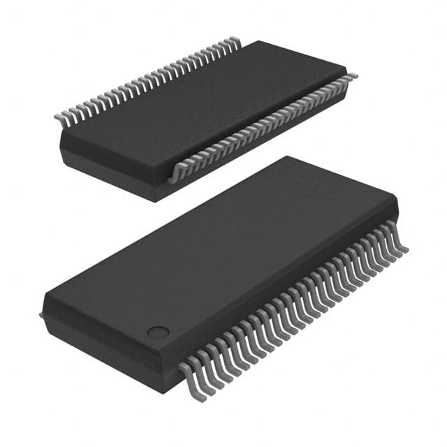
The 74ALVT162821DL,518 is available in a small outline integrated circuit (SOIC) package.
Essence
This IC serves as a versatile interface between different components within a digital system, enabling efficient data transfer and processing.
Packaging/Quantity
The 74ALVT162821DL,518 is typically packaged in reels or tubes, with each reel/tube containing a specific quantity of ICs. The exact quantity may vary depending on the manufacturer's specifications.
Specifications
- Logic family: ALVT
- Number of bits: 16
- Number of input/output pins: 48
- Supply voltage range: 2.3V to 3.6V
- Operating temperature range: -40°C to +85°C
- Input/output voltage levels: CMOS/TTL compatible
Detailed Pin Configuration
The 74ALVT162821DL,518 features a total of 48 pins, which are assigned specific functions. The pin configuration is as follows:
- Pin 1: Output Enable (OE)
- Pin 2: Data Input/Output (DQ0)
- Pin 3: Data Input/Output (DQ1)
- Pin 4: Data Input/Output (DQ2)
- Pin 5: Data Input/Output (DQ3)
- Pin 6: Data Input/Output (DQ4)
- Pin 7: Data Input/Output (DQ5)
- Pin 8: Data Input/Output (DQ6)
- Pin 9: Data Input/Output (DQ7)
- Pin 10: Data Input/Output (DQ8)
- Pin 11: Data Input/Output (DQ9)
- Pin 12: Data Input/Output (DQ10)
- Pin 13: Data Input/Output (DQ11)
- Pin 14: Data Input/Output (DQ12)
- Pin 15: Data Input/Output (DQ13)
- Pin 16: Data Input/Output (DQ14)
- Pin 17: Data Input/Output (DQ15)
- Pin 18: Output Enable (OE)
- Pin 19: Output Enable (OE)
- Pin 20: Output Enable (OE)
- Pin 21: Output Enable (OE)
- Pin 22: Output Enable (OE)
- Pin 23: Output Enable (OE)
- Pin 24: Output Enable (OE)
- Pin 25: Output Enable (OE)
- Pin 26: Output Enable (OE)
- Pin 27: Output Enable (OE)
- Pin 28: Output Enable (OE)
- Pin 29: Output Enable (OE)
- Pin 30: Output Enable (OE)
- Pin 31: Output Enable (OE)
- Pin 32: Output Enable (OE)
- Pin 33: Output Enable (OE)
- Pin 34: Output Enable (OE)
- Pin 35: Output Enable (OE)
- Pin 36: Output Enable (OE)
- Pin 37: Output Enable (OE)
- Pin 38: Output Enable (OE)
- Pin 39: Output Enable (OE)
- Pin 40: Output Enable (OE)
- Pin 41: Output Enable (OE)
- Pin 42: Output Enable (OE)
- Pin 43: Output Enable (OE)
- Pin 44: Output Enable (OE)
- Pin 45: Output Enable (OE)
- Pin 46: Output Enable (OE)
- Pin 47: Output Enable (OE)
- Pin 48: Ground (GND)
Functional Features
The 74ALVT162821DL,518 offers the following functional features:
- Bidirectional data transfer capability
- Output enable control for efficient power management
- High-speed operation for quick data processing
- Compatibility with various logic families, allowing seamless integration into existing systems
- Robustness against noise and interference, ensuring reliable data transmission
Advantages and Disadvantages
Advantages
- High-speed operation enables rapid data processing.
- Low power consumption contributes to energy efficiency.
- Wide operating voltage
기술 솔루션에 74ALVT162821DL,518 적용과 관련된 10가지 일반적인 질문과 답변을 나열하세요.
Sure! Here are 10 common questions and answers related to the application of 74ALVT162821DL,518 in technical solutions:
Q: What is the function of the 74ALVT162821DL,518? A: The 74ALVT162821DL,518 is a 20-bit buffer/driver with 3-state outputs designed for driving highly capacitive or relatively low-impedance loads.
Q: What is the maximum operating voltage for the 74ALVT162821DL,518? A: The maximum operating voltage for the 74ALVT162821DL,518 is 3.6V.
Q: Can the 74ALVT162821DL,518 be used in both input and output applications? A: Yes, the 74ALVT162821DL,518 can be used as both an input buffer and an output driver.
Q: What is the maximum output current that the 74ALVT162821DL,518 can drive? A: The 74ALVT162821DL,518 can drive up to 24mA of current per output.
Q: Is the 74ALVT162821DL,518 compatible with TTL logic levels? A: Yes, the 74ALVT162821DL,518 is compatible with both TTL and CMOS logic levels.
Q: Does the 74ALVT162821DL,518 have internal pull-up or pull-down resistors? A: No, the 74ALVT162821DL,518 does not have internal pull-up or pull-down resistors.
Q: What is the propagation delay of the 74ALVT162821DL,518? A: The propagation delay of the 74ALVT162821DL,518 is typically 3.5ns.
Q: Can the 74ALVT162821DL,518 be used in high-speed applications? A: Yes, the 74ALVT162821DL,518 is designed for high-speed operation and can be used in such applications.
Q: Does the 74ALVT162821DL,518 have thermal shutdown protection? A: No, the 74ALVT162821DL,518 does not have thermal shutdown protection.
Q: What package options are available for the 74ALVT162821DL,518? A: The 74ALVT162821DL,518 is available in a 56-pin TSSOP package.
Please note that these answers are general and may vary depending on the specific datasheet and manufacturer's specifications of the 74ALVT162821DL,518.