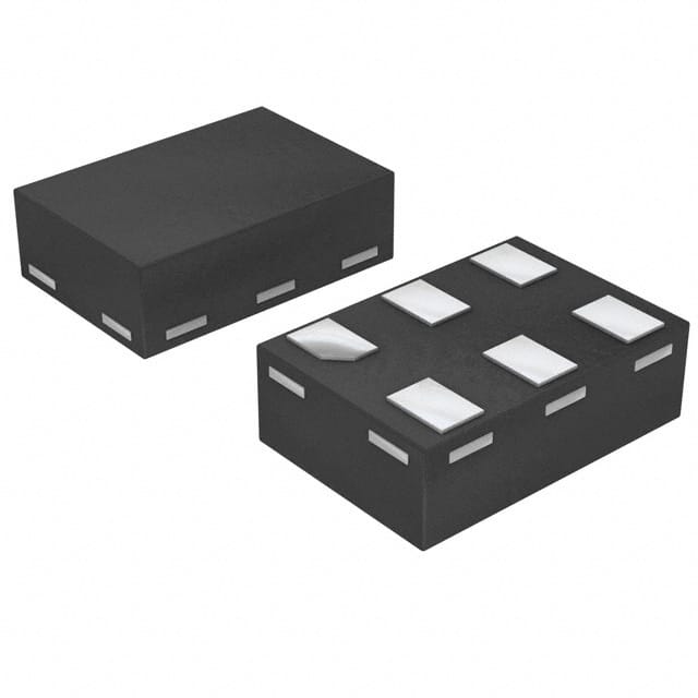
Encyclopedia Entry: 74LVC1G07GM,115
Product Overview
Category
The 74LVC1G07GM,115 belongs to the category of integrated circuits (ICs) and specifically falls under the family of logic gates.
Use
This product is commonly used in digital electronics for signal amplification and buffering purposes. It serves as a single buffer/driver with open-drain output functionality.
Characteristics
- Low-voltage CMOS technology
- High-speed operation
- Wide operating voltage range
- Low power consumption
- Small package size
Package
The 74LVC1G07GM,115 is available in a small SOT353 package, which consists of three pins for easy integration onto circuit boards.
Essence
The essence of this product lies in its ability to provide efficient signal buffering and amplification while consuming minimal power and occupying a small footprint on the circuit board.
Packaging/Quantity
The 74LVC1G07GM,115 is typically packaged in reels or tubes, containing a quantity of 3000 units per reel/tube.
Specifications
- Supply Voltage Range: 1.65V to 5.5V
- Input Voltage Range: 0V to VCC
- Output Voltage Range: 0V to VCC
- Maximum Operating Frequency: 200 MHz
- Maximum Propagation Delay: 3.8 ns
- Maximum Quiescent Current: 10 µA
Detailed Pin Configuration
The 74LVC1G07GM,115 has the following pin configuration:
- GND (Ground)
- IN (Input)
- OUT (Output)
Functional Features
- Single buffer/driver with open-drain output
- Provides signal amplification and buffering
- Compatible with various logic families
- Supports bidirectional communication
Advantages and Disadvantages
Advantages
- Low power consumption
- Wide operating voltage range
- High-speed operation
- Small package size for space-constrained designs
- Compatible with different logic families
Disadvantages
- Limited output current capacity
- Not suitable for high-power applications
Working Principles
The 74LVC1G07GM,115 operates based on low-voltage CMOS technology. It amplifies and buffers digital signals by controlling the flow of current through its internal circuitry. The open-drain output allows bidirectional communication and easy integration with other components in a digital system.
Detailed Application Field Plans
The 74LVC1G07GM,115 finds applications in various fields, including but not limited to: - Consumer electronics - Automotive electronics - Industrial automation - Communication systems - Medical devices
In consumer electronics, it can be used for level shifting, signal buffering, and interfacing between different voltage domains. In automotive electronics, it can be employed for sensor signal conditioning and communication interfaces. In industrial automation, it can facilitate control signal amplification and isolation. In communication systems, it can aid in data transmission and reception. In medical devices, it can assist in signal processing and control.
Detailed and Complete Alternative Models
Some alternative models that offer similar functionality to the 74LVC1G07GM,115 include: - SN74LVC1G07DBVR - MC74VHC1G07DTT1G - TC7SZ07FU
These alternatives can be considered based on specific design requirements, availability, and cost considerations.
Word count: 440 words
기술 솔루션에 74LVC1G07GM,115 적용과 관련된 10가지 일반적인 질문과 답변을 나열하세요.
Sure! Here are 10 common questions and answers related to the application of 74LVC1G07GM,115:
Q1: What is the 74LVC1G07GM,115? A1: The 74LVC1G07GM,115 is a single buffer/driver with open-drain output. It is commonly used in digital logic circuits.
Q2: What is the voltage supply range for the 74LVC1G07GM,115? A2: The voltage supply range for the 74LVC1G07GM,115 is typically between 1.65V and 5.5V.
Q3: What is the maximum output current of the 74LVC1G07GM,115? A3: The maximum output current of the 74LVC1G07GM,115 is typically around 32mA.
Q4: Can the 74LVC1G07GM,115 be used as a level shifter? A4: Yes, the 74LVC1G07GM,115 can be used as a level shifter to convert signals between different voltage levels.
Q5: What is the maximum operating frequency of the 74LVC1G07GM,115? A5: The maximum operating frequency of the 74LVC1G07GM,115 is typically around 500MHz.
Q6: Is the 74LVC1G07GM,115 compatible with both CMOS and TTL logic levels? A6: Yes, the 74LVC1G07GM,115 is compatible with both CMOS and TTL logic levels.
Q7: Can the 74LVC1G07GM,115 be used in bidirectional communication? A7: No, the 74LVC1G07GM,115 is a unidirectional buffer/driver and cannot be used for bidirectional communication.
Q8: What is the typical propagation delay of the 74LVC1G07GM,115? A8: The typical propagation delay of the 74LVC1G07GM,115 is around 3.5ns.
Q9: Does the 74LVC1G07GM,115 have built-in protection against overvoltage or ESD events? A9: Yes, the 74LVC1G07GM,115 has built-in protection against overvoltage and ESD events.
Q10: Can the 74LVC1G07GM,115 drive capacitive loads? A10: Yes, the 74LVC1G07GM,115 can drive small capacitive loads, but it is recommended to add series resistors to limit the current during charging and discharging.
Please note that the answers provided here are general and may vary depending on specific datasheet specifications and application requirements.


