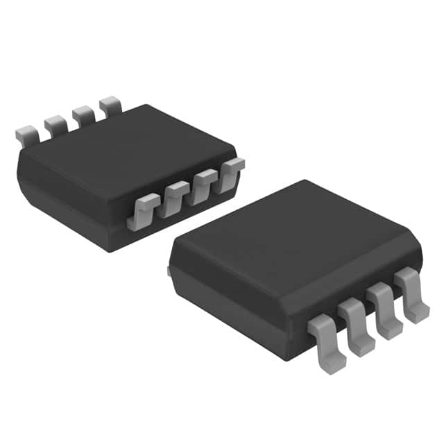
74LVC2G126DC,125
Basic Information Overview
- Category: Integrated Circuit (IC)
- Use: Logic Level Shifter
- Characteristics: Dual Bus Buffer Gate with 3-State Outputs
- Package: VSSOP (Very Small Outline Package)
- Essence: This IC is designed to shift logic levels between two different voltage domains, allowing communication between devices operating at different voltage levels.
- Packaging/Quantity: Available in tape and reel packaging, with a quantity of 3000 units per reel.
Specifications
- Supply Voltage Range: 1.65V to 5.5V
- High-Level Input Voltage: 0.7 x VCC
- Low-Level Input Voltage: 0.3 x VCC
- High-Level Output Voltage: 0.9 x VCC
- Low-Level Output Voltage: 0.1 x VCC
- Maximum Operating Frequency: 400 MHz
- Maximum Propagation Delay: 4.6 ns
Detailed Pin Configuration
The 74LVC2G126DC,125 has a total of 8 pins: 1. Pin 1: A Input 2. Pin 2: Y Output 3. Pin 3: OE (Output Enable) Input 4. Pin 4: GND (Ground) 5. Pin 5: B Input 6. Pin 6: Y Output 7. Pin 7: VCC (Supply Voltage) 8. Pin 8: GND (Ground)
Functional Features
- Dual Bus Buffer Gate: Allows bidirectional signal transfer between two buses.
- 3-State Outputs: The outputs can be put into a high-impedance state, enabling multiple devices to share the same bus without interference.
- Wide Supply Voltage Range: Supports operation from 1.65V to 5.5V, making it compatible with various voltage domains.
- High-Speed Operation: Capable of operating at frequencies up to 400 MHz, ensuring efficient data transfer.
Advantages and Disadvantages
Advantages: - Enables communication between devices with different voltage levels. - Supports bidirectional signal transfer. - Allows multiple devices to share the same bus without interference. - Wide supply voltage range provides flexibility in system design. - High-speed operation ensures efficient data transfer.
Disadvantages: - Limited maximum propagation delay may not be suitable for applications requiring precise timing. - VSSOP package may require careful handling during assembly.
Working Principles
The 74LVC2G126DC,125 operates by receiving input signals from two different voltage domains, A and B. It then shifts the logic levels of these signals to match the desired output voltage level, Y. The OE (Output Enable) input controls the output state, allowing the outputs to be either active or in a high-impedance state.
Detailed Application Field Plans
The 74LVC2G126DC,125 is commonly used in various applications where logic level shifting is required. Some potential application fields include: 1. Communication Systems: Facilitating communication between devices operating at different voltage levels, such as microcontrollers and sensors. 2. Industrial Automation: Enabling compatibility between different components within automation systems. 3. Consumer Electronics: Supporting interconnection between devices with varying voltage requirements, like smartphones and peripherals. 4. Automotive Electronics: Ensuring seamless communication between different subsystems in vehicles.
Detailed and Complete Alternative Models
Some alternative models that offer similar functionality to the 74LVC2G126DC,125 are: - SN74LVC2G126DCTR: Dual Bus Buffer Gate with 3-State Outputs, available in a smaller SOT-23 package. - MC74LVC2G126DTG: Dual Bus Buffer Gate with 3-State Outputs, featuring a wider supply voltage range. - TC7SZ126AFK: Single Bus Buffer Gate with 3-State Output, suitable for applications requiring a single buffer.
(Note: The above alternative models are provided for reference and may have slight variations in specifications and pin configuration. It is recommended to consult the respective datasheets for detailed information.)
Word count: 536 words
기술 솔루션에 74LVC2G126DC,125 적용과 관련된 10가지 일반적인 질문과 답변을 나열하세요.
Sure! Here are 10 common questions and answers related to the application of 74LVC2G126DC,125 in technical solutions:
Q: What is the function of the 74LVC2G126DC,125? A: The 74LVC2G126DC,125 is a dual bus buffer/line driver with 3-state outputs. It can be used to control the flow of data between two buses or systems.
Q: What is the operating voltage range of the 74LVC2G126DC,125? A: The operating voltage range is from 1.65V to 5.5V.
Q: Can the 74LVC2G126DC,125 handle high-speed data transmission? A: Yes, it is designed for high-speed operation and can support data rates up to 400 Mbps.
Q: How many output pins does the 74LVC2G126DC,125 have? A: It has two output pins, one for each buffer.
Q: What is the maximum output current that the 74LVC2G126DC,125 can provide? A: The maximum output current is typically 24 mA.
Q: Can the 74LVC2G126DC,125 be used in both digital and analog applications? A: No, it is specifically designed for digital applications and may not perform well in analog circuits.
Q: Is the 74LVC2G126DC,125 compatible with other logic families? A: Yes, it is compatible with both CMOS and TTL logic levels.
Q: Does the 74LVC2G126DC,125 have built-in protection features? A: Yes, it has built-in ESD protection to prevent damage from electrostatic discharge.
Q: Can the 74LVC2G126DC,125 be used in battery-powered applications? A: Yes, it has a low power consumption and can be used in battery-powered devices.
Q: Are there any specific layout considerations for using the 74LVC2G126DC,125? A: Yes, it is recommended to follow the manufacturer's guidelines for proper PCB layout and decoupling capacitor placement to ensure optimal performance.
Please note that these answers are general and may vary depending on the specific application and requirements. It is always recommended to refer to the datasheet and consult with an expert when designing technical solutions.


