

74LVC2G38GD,125
Basic Information Overview
- Category: Integrated Circuit (IC)
- Use: Logic Gate
- Characteristics: Dual 2-input NAND gate with Schmitt-trigger inputs
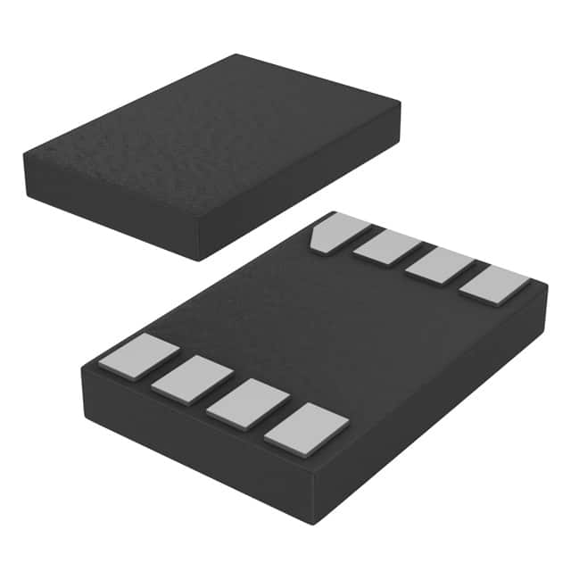
- Package: VSSOP8
- Essence: High-speed CMOS technology
- Packaging/Quantity: Tape and Reel, 3000 pieces per reel
Specifications
- Supply Voltage Range: 1.65V to 5.5V
- Input Voltage Range: -0.5V to 7V
- Output Voltage Range: 0V to VCC
- Operating Temperature Range: -40°C to +125°C
- Propagation Delay: 3.9ns (typical) at 3.3V supply voltage
Detailed Pin Configuration
The 74LVC2G38GD,125 has a VSSOP8 package with the following pin configuration:
___________
   1 |           | 8
   2 |           | 7
   3 |           | 6
   4 |           | 5
     |___________|
Pin Description: 1. A Input 1 2. B Input 2 3. Y Output 4. GND Ground 5. Y Output 6. B Input 2 7. A Input 1 8. VCC Power Supply
Functional Features
- Dual 2-input NAND gate with Schmitt-trigger inputs
- Schmitt-trigger inputs allow for hysteresis and improved noise immunity
- High-speed operation suitable for various applications
- Low power consumption
- Compatible with both TTL and CMOS logic levels
- Wide operating voltage range
Advantages and Disadvantages
Advantages: - High-speed operation - Improved noise immunity due to Schmitt-trigger inputs - Wide operating voltage range allows for compatibility with various systems - Low power consumption
Disadvantages: - Limited number of inputs (dual 2-input NAND gate) - Relatively small package size may require careful handling during assembly
Working Principles
The 74LVC2G38GD,125 is a dual 2-input NAND gate with Schmitt-trigger inputs. It operates based on the principles of complementary metal-oxide-semiconductor (CMOS) technology. The Schmitt-trigger inputs provide hysteresis, which helps in reducing noise and improving the stability of the output signal. When both input signals are low, the output is high. Otherwise, the output is low.
Detailed Application Field Plans
The 74LVC2G38GD,125 can be used in various applications that require logic gate functionality. Some potential application fields include: - Digital signal processing - Communication systems - Industrial automation - Consumer electronics - Automotive electronics
Detailed and Complete Alternative Models
Some alternative models to the 74LVC2G38GD,125 that offer similar functionality include: - SN74LVC2G38DBVR by Texas Instruments - MC74VHC1G00DTT1G by ON Semiconductor - CD4011BM96 by Texas Instruments - HCF4011BEY by STMicroelectronics
Note: This list is not exhaustive and there are other alternative models available in the market.
Word count: 346 words
기술 솔루션에 74LVC2G38GD,125 적용과 관련된 10가지 일반적인 질문과 답변을 나열하세요.
Sure! Here are 10 common questions and answers related to the application of 74LVC2G38GD,125 in technical solutions:
Q: What is the function of the 74LVC2G38GD,125? A: The 74LVC2G38GD,125 is a dual 2-input NAND gate with Schmitt-trigger inputs.
Q: What is the operating voltage range for the 74LVC2G38GD,125? A: The operating voltage range is from 1.65V to 5.5V.
Q: Can the 74LVC2G38GD,125 be used in both digital and analog applications? A: No, it is primarily designed for digital applications.
Q: What is the maximum output current of the 74LVC2G38GD,125? A: The maximum output current is typically 32mA.
Q: Does the 74LVC2G38GD,125 have built-in protection against electrostatic discharge (ESD)? A: Yes, it has ESD protection up to 2kV.
Q: Can I use the 74LVC2G38GD,125 in high-speed applications? A: Yes, it is suitable for high-speed operation with propagation delays as low as 3.8ns.
Q: Is the 74LVC2G38GD,125 compatible with other logic families? A: It is compatible with both CMOS and TTL logic families.
Q: What is the power supply current consumption of the 74LVC2G38GD,125? A: The typical power supply current is around 0.9mA.
Q: Can I use the 74LVC2G38GD,125 in battery-powered applications? A: Yes, it is suitable for battery-powered devices due to its low power consumption.
Q: Are there any specific precautions to consider when using the 74LVC2G38GD,125? A: It is recommended to avoid exceeding the maximum operating voltage and to follow proper ESD handling procedures.
Please note that these answers are general and may vary depending on the specific datasheet and application requirements of the 74LVC2G38GD,125.