

74LVCH162374ADL:11
Basic Information Overview
- Category: Integrated Circuit (IC)
- Use: Logic Level Shifter
- Characteristics: High-speed, low-power, non-inverting, 16-bit, 3.3V to 5V voltage translation
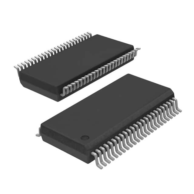
- Package: TSSOP (Thin Shrink Small Outline Package)
- Essence: Bi-directional voltage level shifting between 3.3V and 5V logic levels
- Packaging/Quantity: Tape and Reel, 2500 units per reel
Specifications
- Supply Voltage Range: 1.2V to 5.5V
- Input Voltage Range: 0V to VCC
- Output Voltage Range: 0V to VCC
- Maximum Operating Frequency: 200 MHz
- Propagation Delay: 4.5 ns (typical)
- Output Drive Capability: ±24 mA
- ESD Protection: Human Body Model > 2000V
Detailed Pin Configuration
The 74LVCH162374ADL:11 IC has a total of 48 pins arranged in a TSSOP package. The pin configuration is as follows:
+-------------------+
   OE --|1                48|-- VCC
  GND --|2                47|-- A1
  D1A --|3                46|-- B1
  D2A --|4                45|-- C1
  D3A --|5                44|-- D1
  D4A --|6                43|-- E1
  D5A --|7                42|-- F1
  D6A --|8                41|-- G1
  D7A --|9                40|-- H1
  D8A --|10               39|-- OE#
  D8B --|11               38|-- GND
  D7B --|12               37|-- A2
  D6B --|13               36|-- B2
  D5B --|14               35|-- C2
  D4B --|15               34|-- D2
  D3B --|16               33|-- E2
  D2B --|17               32|-- F2
  D1B --|18               31|-- G2
   LE --|19               30|-- H2
  CLK --|20               29|-- LE#
  GND --|21               28|-- GND
  Q1A --|22               27|-- Q1B
  Q2A --|23               26|-- Q2B
  Q3A --|24               25|-- Q3B
        +-------------------+
Functional Features
- Bi-directional voltage level shifting: Allows seamless translation between 3.3V and 5V logic levels.
- Non-inverting: The input signal is not inverted at the output.
- High-speed operation: Supports a maximum operating frequency of 200 MHz.
- Low-power consumption: Designed to minimize power consumption during operation.
- Output drive capability: Can drive up to ±24 mA of current for robust signal transmission.
- ESD protection: Provides protection against electrostatic discharge, ensuring device reliability.
Advantages and Disadvantages
Advantages: - Enables easy interfacing between different logic voltage levels. - High-speed operation allows for efficient data transfer. - Low-power consumption helps in reducing overall system power requirements. - Robust output drive capability ensures reliable signal transmission. - ESD protection enhances device durability.
Disadvantages: - Limited to voltage translation between 3.3V and 5V logic levels. - May not be suitable for applications requiring voltage translation beyond the specified range.
Working Principles
The 74LVCH162374ADL:11 is a logic level shifter that utilizes a combination of MOSFETs to achieve bi-directional voltage translation between 3.3V and 5V logic levels. The input signal is non-inverted at the output, ensuring seamless data transfer. The IC operates at high speed while consuming low power, making it suitable for various applications.
Detailed Application Field Plans
The 74LVCH162374ADL:11 finds application in various fields, including but not limited to: - Microcontroller interfacing with different voltage levels - Communication systems involving multiple logic standards - Data transmission between devices operating at different voltage levels - Industrial automation and control systems - Consumer electronics
Detailed and Complete Alternative Models
Some alternative models that provide similar functionality to the 74LVCH162374ADL:11 are: - SN74LVC1T45: Single-bit, bi-directional voltage level translator - TXB0108:
기술 솔루션에 74LVCH162374ADL:11 적용과 관련된 10가지 일반적인 질문과 답변을 나열하세요.
Sure! Here are 10 common questions and answers related to the application of 74LVCH162374ADL:11 in technical solutions:
Q: What is the function of the 74LVCH162374ADL:11? A: The 74LVCH162374ADL:11 is a 16-bit D-type flip-flop with 3-state outputs, designed for low-voltage applications.
Q: What is the voltage range supported by the 74LVCH162374ADL:11? A: The 74LVCH162374ADL:11 supports a voltage range of 1.65V to 5.5V.
Q: How many flip-flops are there in the 74LVCH162374ADL:11? A: The 74LVCH162374ADL:11 has 16 individual flip-flops.
Q: What is the purpose of the 3-state outputs in the 74LVCH162374ADL:11? A: The 3-state outputs allow multiple devices to share a common bus without interfering with each other.
Q: Can the 74LVCH162374ADL:11 be used in high-speed applications? A: Yes, the 74LVCH162374ADL:11 is designed for high-speed operation, making it suitable for various applications.
Q: What is the maximum operating frequency of the 74LVCH162374ADL:11? A: The maximum operating frequency of the 74LVCH162374ADL:11 is typically around 200 MHz.
Q: Does the 74LVCH162374ADL:11 have any built-in protection features? A: Yes, the 74LVCH162374ADL:11 has built-in ESD protection, which helps safeguard against electrostatic discharge.
Q: Can the 74LVCH162374ADL:11 be used in both input and output applications? A: Yes, the 74LVCH162374ADL:11 can be used as both an input and output device, depending on the specific application requirements.
Q: What is the power supply voltage range for the 74LVCH162374ADL:11? A: The power supply voltage range for the 74LVCH162374ADL:11 is typically between 1.65V and 3.6V.
Q: Are there any special considerations when designing with the 74LVCH162374ADL:11? A: It is important to ensure proper decoupling capacitors are used near the power supply pins to minimize noise and ensure stable operation.
Please note that these answers are general and may vary depending on the specific datasheet and application guidelines provided by the manufacturer of the 74LVCH162374ADL:11.