

74LVT16373ADL,118
Basic Information Overview
- Category: Integrated Circuit (IC)
- Use: Data storage and transfer
- Characteristics: High-speed, low-voltage, transparent latch
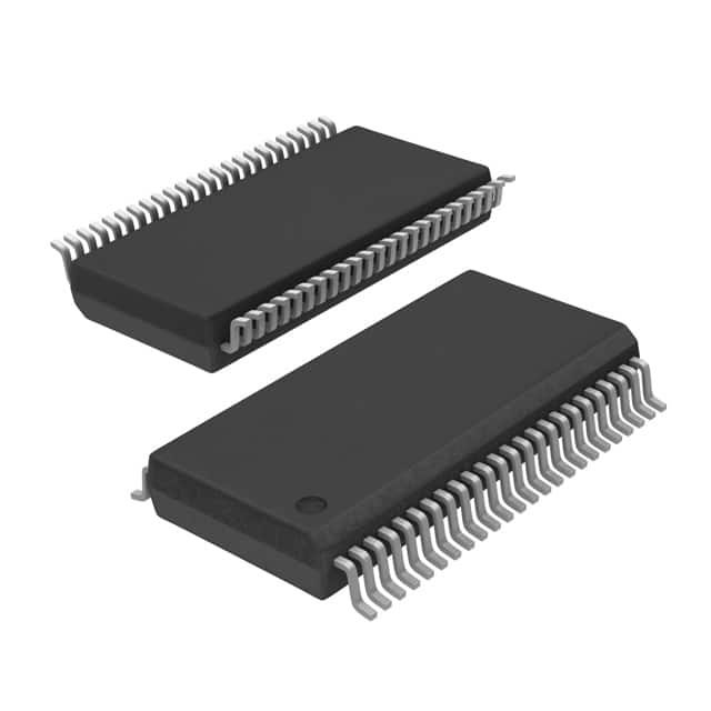
- Package: TSSOP (Thin Shrink Small Outline Package)
- Essence: Transparent D-type latch with 16-bit capacity
- Packaging/Quantity: Tape and reel, 2500 units per reel
Specifications
- Logic Family: LVT (Low Voltage TTL)
- Number of Bits: 16
- Supply Voltage: 2.7V to 3.6V
- Input Voltage Levels: CMOS/TTL compatible
- Output Voltage Levels: CMOS/TTL compatible
- Operating Temperature Range: -40°C to +85°C
- Propagation Delay Time: 4.5 ns (typical)
- Output Drive Capability: ±24 mA
Detailed Pin Configuration
The 74LVT16373ADL,118 IC has a total of 48 pins. The pin configuration is as follows:
- Pin 1: Output Enable (OE) for latch 1
- Pin 2: Data Input (D1) for latch 1
- Pin 3: Clock Input (CP1) for latch 1
- Pin 4: Clock Enable (CE1) for latch 1
- Pin 5: GND (Ground)
- Pin 6: Q1 Output for latch 1
- Pin 7: Q̅1 Output for latch 1
- Pin 8: VCC (Supply Voltage)
- Pin 9: Q̅2 Output for latch 2
- Pin 10: Q2 Output for latch 2
- Pin 11: CE2 Clock Enable for latch 2
- Pin 12: CP2 Clock Input for latch 2
- Pin 13: D2 Data Input for latch 2
- Pin 14: OE Output Enable for latch 2
- Pin 15: GND (Ground)
- Pin 16: Q3 Output for latch 3
- Pin 17: Q̅3 Output for latch 3
- Pin 18: VCC (Supply Voltage)
- Pin 19: Q̅4 Output for latch 4
- Pin 20: Q4 Output for latch 4
- Pin 21: CE3 Clock Enable for latch 3
- Pin 22: CP3 Clock Input for latch 3
- Pin 23: D3 Data Input for latch 3
- Pin 24: OE Output Enable for latch 3
- Pin 25: GND (Ground)
- Pin 26: Q5 Output for latch 5
- Pin 27: Q̅5 Output for latch 5
- Pin 28: VCC (Supply Voltage)
- Pin 29: Q̅6 Output for latch 6
- Pin 30: Q6 Output for latch 6
- Pin 31: CE4 Clock Enable for latch 4
- Pin 32: CP4 Clock Input for latch 4
- Pin 33: D4 Data Input for latch 4
- Pin 34: OE Output Enable for latch 4
- Pin 35: GND (Ground)
- Pin 36: Q7 Output for latch 7
- Pin 37: Q̅7 Output for latch 7
- Pin 38: VCC (Supply Voltage)
- Pin 39: Q̅8 Output for latch 8
- Pin 40: Q8 Output for latch 8
- Pin 41: CE5 Clock Enable for latch 5
- Pin 42: CP5 Clock Input for latch 5
- Pin 43: D5 Data Input for latch 5
- Pin 44: OE Output Enable for latch 5
- Pin 45: GND (Ground)
- Pin 46: Q9 Output for latch 9
- Pin 47: Q̅9 Output for latch 9
- Pin 48: VCC (Supply Voltage)
Functional Features
- Transparent latch operation allows real-time data transfer
- High-speed performance suitable for applications requiring quick data storage and retrieval
- Low-voltage operation makes it compatible with modern electronic systems
- Multiple latch configurations provide flexibility in data handling
Advantages and Disadvantages
Advantages: - High-speed operation enables efficient data transfer - Low-voltage design reduces power consumption - Compact TSSOP package saves board space - Compatibility with CM
기술 솔루션에 74LVT16373ADL,118 적용과 관련된 10가지 일반적인 질문과 답변을 나열하세요.
Sure! Here are 10 common questions and answers related to the application of 74LVT16373ADL,118 in technical solutions:
Q: What is the function of the 74LVT16373ADL,118? A: The 74LVT16373ADL,118 is a 16-bit transparent latch with 3-state outputs. It can be used for temporary storage or data buffering.
Q: What is the maximum operating voltage for the 74LVT16373ADL,118? A: The maximum operating voltage for this device is typically 3.6V.
Q: Can I use the 74LVT16373ADL,118 in a 5V system? A: No, this device is not compatible with 5V systems as its maximum voltage is 3.6V. You would need a level-shifting circuit to interface it with a 5V system.
Q: How many latch outputs does the 74LVT16373ADL,118 have? A: This device has 16 latch outputs, corresponding to the 16 input lines.
Q: What is the output drive capability of the 74LVT16373ADL,118? A: The output drive capability is typically 32mA, which allows it to drive standard CMOS or TTL loads.
Q: Can I connect multiple 74LVT16373ADL,118 devices together? A: Yes, you can connect multiple devices together to increase the number of latch outputs or create larger storage arrays.
Q: Does the 74LVT16373ADL,118 have any internal pull-up or pull-down resistors? A: No, this device does not have internal pull-up or pull-down resistors. External resistors may be required for proper operation.
Q: What is the propagation delay of the 74LVT16373ADL,118? A: The typical propagation delay is around 4.5ns, but it can vary depending on the operating conditions.
Q: Can I use the 74LVT16373ADL,118 in high-speed applications? A: Yes, this device is designed for high-speed operation and can be used in applications with fast data transfer rates.
Q: Is the 74LVT16373ADL,118 compatible with other logic families? A: Yes, this device is compatible with a wide range of logic families, including CMOS, TTL, and LVTTL.
Please note that these answers are general and may vary depending on the specific datasheet and manufacturer's specifications for the 74LVT16373ADL,118.