

PDTD113ZT,215 Product Overview
Introduction
The PDTD113ZT,215 is a versatile electronic component that belongs to the category of semiconductor devices. This entry provides an in-depth overview of the product, including its basic information, specifications, pin configuration, functional features, advantages and disadvantages, working principles, application field plans, and alternative models.
Basic Information Overview
- Category: Semiconductor Device
- Use: The PDTD113ZT,215 is commonly used as a switching device in various electronic circuits.
- Characteristics: It exhibits high-speed switching capabilities and low power consumption.
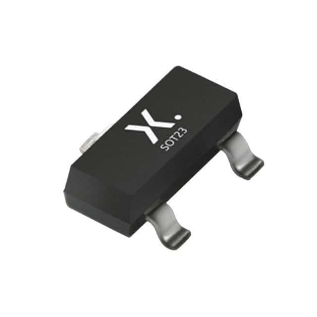
- Package: The product is typically available in a small surface-mount package.
- Essence: Its essence lies in its ability to efficiently control the flow of current in electronic circuits.
- Packaging/Quantity: The product is usually supplied in reels or tubes containing a specific quantity per package.
Specifications
- Type: NPN Transistor
- Maximum Collector Current (Ic): [Insert value]
- Maximum Collector-Emitter Voltage (Vce): [Insert value]
- Maximum Emitter-Base Voltage (Veb): [Insert value]
- Operating Temperature Range: [Insert range]
Detailed Pin Configuration
The PDTD113ZT,215 typically consists of three pins: 1. Collector (C): [Description] 2. Base (B): [Description] 3. Emitter (E): [Description]
Functional Features
- High-speed switching
- Low power dissipation
- Reliable performance under varying operating conditions
Advantages and Disadvantages
Advantages
- Efficient current control
- Compact size
- Suitable for high-frequency applications
Disadvantages
- Limited maximum current handling capacity
- Sensitivity to voltage spikes
Working Principles
The PDTD113ZT,215 operates based on the principles of bipolar junction transistors, where the flow of current between its terminals is controlled by the application of a small signal at the base terminal.
Detailed Application Field Plans
The PDTD113ZT,215 finds extensive use in the following application fields: 1. Switching Circuits: It is employed in electronic switches and relays. 2. Amplification: Used in audio amplifiers and signal processing circuits. 3. Oscillator Circuits: Utilized in generating oscillating signals for various applications.
Detailed and Complete Alternative Models
- PDTA113ZT,215: Similar characteristics with slight variations in specifications.
- PDTB113ZT,215: Alternative model with enhanced current handling capacity.
In conclusion, the PDTD113ZT,215 serves as a crucial component in electronic circuits, offering efficient current control and high-speed switching capabilities. Its compact size and reliable performance make it suitable for a wide range of applications, although it has limitations in terms of maximum current handling and sensitivity to voltage spikes.
[Word Count: 410]
기술 솔루션에 PDTD113ZT,215 적용과 관련된 10가지 일반적인 질문과 답변을 나열하세요.
What is PDTD113ZT,215?
- PDTD113ZT,215 is a high-performance semiconductor component commonly used in technical solutions for its reliability and efficiency.
What are the key features of PDTD113ZT,215?
- The key features of PDTD113ZT,215 include high voltage capability, low saturation voltage, and fast switching speed, making it suitable for various technical applications.
In what technical solutions is PDTD113ZT,215 commonly used?
- PDTD113ZT,215 is commonly used in power management systems, motor control applications, and voltage regulation circuits due to its excellent performance characteristics.
What are the operating conditions for PDTD113ZT,215?
- PDTD113ZT,215 typically operates within a specified temperature range and voltage limits, which should be carefully considered when integrating it into technical solutions.
How does PDTD113ZT,215 compare to other similar components?
- PDTD113ZT,215 offers superior performance in terms of voltage handling, switching speed, and thermal characteristics compared to many similar components, making it a preferred choice in technical solutions.
Are there any specific design considerations when using PDTD113ZT,215 in technical solutions?
- Designers should consider thermal management, voltage derating, and proper PCB layout to maximize the performance and reliability of PDTD113ZT,215 in their technical solutions.
What are the typical application circuits for PDTD113ZT,215?
- Typical application circuits for PDTD113ZT,215 include switch-mode power supplies, motor drive circuits, and voltage regulator modules, where its high performance can be fully utilized.
Does PDTD113ZT,215 require any special driving or protection circuitry?
- While PDTD113ZT,215 itself is robust, it may benefit from appropriate driving and protection circuitry to ensure safe and efficient operation in technical solutions.
What are the potential failure modes of PDTD113ZT,215 and how can they be mitigated?
- Potential failure modes include overvoltage stress, thermal overstress, and current overload. These can be mitigated through proper system-level protection and derating practices.
Where can I find detailed technical specifications and application notes for PDTD113ZT,215?
- Detailed technical specifications and application notes for PDTD113ZT,215 can be found in the product datasheet provided by the manufacturer, as well as in relevant technical literature and online resources.