

74LVT2952PW,112
Basic Information Overview
- Category: Integrated Circuit (IC)
- Use: Multiplexer/Demultiplexer
- Characteristics: Low Voltage, High-Speed, Tri-State Outputs
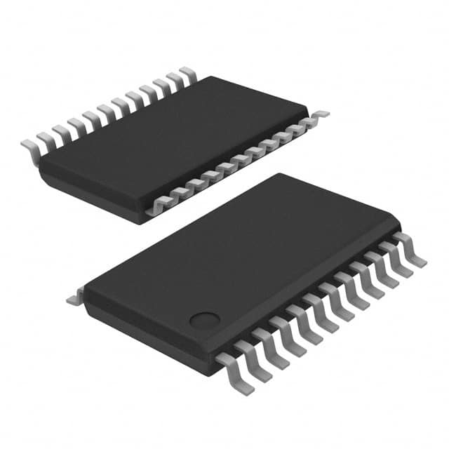
- Package: TSSOP (Thin Shrink Small Outline Package)
- Essence: Logic Level Translator
- Packaging/Quantity: Tape and Reel, 2500 pieces per reel
Specifications
- Supply Voltage Range: 1.2V to 3.6V
- Input Voltage Range: -0.5V to VCC + 0.5V
- Output Voltage Range: 0V to VCC
- Maximum Operating Frequency: 200MHz
- Number of Channels: 8
Detailed Pin Configuration
The 74LVT2952PW,112 has a total of 20 pins. The pin configuration is as follows:
Pin 1: Channel 0 Data Input
Pin 2: Channel 1 Data Input
Pin 3: Channel 2 Data Input
Pin 4: Channel 3 Data Input
Pin 5: Channel 4 Data Input
Pin 6: Channel 5 Data Input
Pin 7: Channel 6 Data Input
Pin 8: Channel 7 Data Input
Pin 9: Enable Input
Pin 10: Channel Select Input
Pin 11: Channel 0 Data Output
Pin 12: Channel 1 Data Output
Pin 13: Channel 2 Data Output
Pin 14: Channel 3 Data Output
Pin 15: Channel 4 Data Output
Pin 16: Channel 5 Data Output
Pin 17: Channel 6 Data Output
Pin 18: Channel 7 Data Output
Pin 19: Ground (GND)
Pin 20: Power Supply (VCC)
Functional Features
- Logic Level Translation: The 74LVT2952PW,112 is designed to translate logic levels between different voltage domains.
- Multiplexing/Demultiplexing: It can be used as an 8-channel multiplexer or demultiplexer, allowing for efficient data routing.
- Tri-State Outputs: The outputs of the IC can be put in a high-impedance state, enabling multiple devices to share a common bus.
Advantages and Disadvantages
Advantages: - Low Voltage Operation: Suitable for low-power applications. - High-Speed Operation: Can handle high-frequency signals. - Tri-State Outputs: Allows for bus sharing and reduces contention issues.
Disadvantages: - Limited Channel Count: Only supports up to 8 channels. - Narrow Supply Voltage Range: May not be compatible with all voltage levels.
Working Principles
The 74LVT2952PW,112 operates by receiving input data on the corresponding channel inputs. The channel select input determines which channel's data is being routed to the output. The enable input controls whether the outputs are active or in a high-impedance state. The IC uses internal circuitry to perform logic level translation and ensure proper signal integrity.
Detailed Application Field Plans
The 74LVT2952PW,112 finds applications in various fields, including: 1. Communication Systems: Used for data routing and signal level translation in communication protocols. 2. Industrial Automation: Enables interfacing between different voltage domains in industrial control systems. 3. Consumer Electronics: Facilitates data multiplexing/demultiplexing in audio/video equipment and gaming consoles. 4. Automotive Electronics: Helps in connecting sensors and actuators operating at different voltage levels in automotive systems.
Detailed and Complete Alternative Models
Some alternative models that offer similar functionality to the 74LVT2952PW,112 include: - SN74LVC8T245PW: 8-bit level translator with similar characteristics and package. - CD74HCT4051M: 8-channel analog multiplexer/demultiplexer with tri-state outputs. - MC74LVX4053DTR2G: Triple 2-channel analog multiplexer/demultiplexer with logic level translation.
(Note: The above alternatives are just a few examples and not an exhaustive list.)
This entry provides comprehensive information about the 74LVT2952PW,112, including its basic overview, specifications, pin configuration, functional features, advantages and disadvantages, working principles, application field plans, and alternative models.
기술 솔루션에 74LVT2952PW,112 적용과 관련된 10가지 일반적인 질문과 답변을 나열하세요.
Sure! Here are 10 common questions and answers related to the application of 74LVT2952PW,112:
Q: What is the function of the 74LVT2952PW,112? A: The 74LVT2952PW,112 is a multiplexer/demultiplexer IC that allows for the selection of one input from multiple sources or the distribution of one input to multiple outputs.
Q: What is the operating voltage range of the 74LVT2952PW,112? A: The operating voltage range of the 74LVT2952PW,112 is typically between 2.7V and 3.6V.
Q: How many inputs and outputs does the 74LVT2952PW,112 have? A: The 74LVT2952PW,112 has 8 inputs and 3 outputs.
Q: Can the 74LVT2952PW,112 handle both analog and digital signals? A: Yes, the 74LVT2952PW,112 can handle both analog and digital signals.
Q: What is the maximum data rate supported by the 74LVT2952PW,112? A: The maximum data rate supported by the 74LVT2952PW,112 is typically around 200MHz.
Q: Does the 74LVT2952PW,112 have any built-in protection features? A: Yes, the 74LVT2952PW,112 has built-in ESD protection on its inputs and outputs.
Q: Can I use the 74LVT2952PW,112 in a high-speed data switching application? A: Yes, the 74LVT2952PW,112 is suitable for high-speed data switching applications due to its low propagation delay and fast switching times.
Q: What is the power consumption of the 74LVT2952PW,112? A: The power consumption of the 74LVT2952PW,112 is typically low, making it suitable for battery-powered devices.
Q: Can I cascade multiple 74LVT2952PW,112 ICs together? A: Yes, you can cascade multiple 74LVT2952PW,112 ICs together to increase the number of inputs or outputs.
Q: Are there any specific layout considerations when using the 74LVT2952PW,112? A: It is recommended to follow proper PCB layout guidelines, such as minimizing trace lengths and ensuring proper decoupling capacitors are used, to optimize performance and minimize noise.
Please note that the answers provided here are general and may vary depending on the specific datasheet and application requirements.