

MC68HC711D3CFNE2
Product Overview
- Category: Microcontroller
- Use: Embedded systems, automotive applications
- Characteristics: High-performance, low-power consumption, versatile
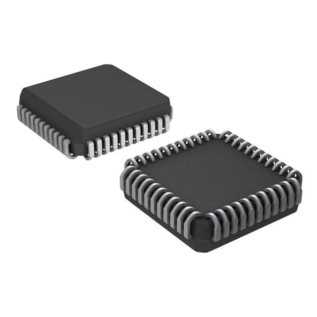
- Package: 52-pin QFP (Quad Flat Package)
- Essence: A powerful microcontroller designed for embedded systems in automotive applications
- Packaging/Quantity: Available in tape and reel packaging, quantity varies based on customer requirements
Specifications
- Architecture: 8-bit
- Clock Speed: Up to 2 MHz
- Program Memory: 16 KB Flash
- RAM: 512 bytes
- I/O Pins: 38
- Timers: 2
- Analog-to-Digital Converter: 8 channels, 8-bit resolution
- Communication Interfaces: UART, SPI, I2C
Pin Configuration
The MC68HC711D3CFNE2 microcontroller has a total of 52 pins. The pin configuration is as follows:
- VDD - Power supply voltage
- VSS - Ground
- PA0 - General-purpose I/O pin
- PA1 - General-purpose I/O pin
- PA2 - General-purpose I/O pin
- PA3 - General-purpose I/O pin
- PA4 - General-purpose I/O pin
- PA5 - General-purpose I/O pin
- PA6 - General-purpose I/O pin
- PA7 - General-purpose I/O pin
- PB0 - General-purpose I/O pin
- PB1 - General-purpose I/O pin
- PB2 - General-purpose I/O pin
- PB3 - General-purpose I/O pin
- PB4 - General-purpose I/O pin
- PB5 - General-purpose I/O pin
- PB6 - General-purpose I/O pin
- PB7 - General-purpose I/O pin
- PC0 - General-purpose I/O pin
- PC1 - General-purpose I/O pin
- PC2 - General-purpose I/O pin
- PC3 - General-purpose I/O pin
- PC4 - General-purpose I/O pin
- PC5 - General-purpose I/O pin
- PC6 - General-purpose I/O pin
- PC7 - General-purpose I/O pin
- PD0 - General-purpose I/O pin
- PD1 - General-purpose I/O pin
- PD2 - General-purpose I/O pin
- PD3 - General-purpose I/O pin
- PD4 - General-purpose I/O pin
- PD5 - General-purpose I/O pin
- PD6 - General-purpose I/O pin
- PD7 - General-purpose I/O pin
- PE0 - General-purpose I/O pin
- PE1 - General-purpose I/O pin
- PE2 - General-purpose I/O pin
- PE3 - General-purpose I/O pin
- PE4 - General-purpose I/O pin
- PE5 - General-purpose I/O pin
- PE6 - General-purpose I/O pin
- PE7 - General-purpose I/O pin
- PF0 - General-purpose I/O pin
- PF1 - General-purpose I/O pin
- PF2 - General-purpose I/O pin
- PF3 - General-purpose I/O pin
- PF4 - General-purpose I/O pin
- PF5 - General-purpose I/O pin
- PF6 - General-purpose I/O pin
- PF7 - General-purpose I/O pin
- RESET - Reset pin
- XTAL - Crystal oscillator input
Functional Features
- High-performance 8-bit microcontroller
- Low-power consumption for efficient operation
- Versatile I/O capabilities with 38 pins
- Integrated timers for precise timing control
- Analog-to-Digital Converter (ADC) for analog signal processing
- Multiple communication interfaces (UART, SPI, I2C) for data exchange
Advantages and Disadvantages
Advantages
- Powerful processing capabilities suitable for demanding applications
- Low power consumption extends battery life in portable devices
- Versatile I/O pins allow for flexible interfacing with external components
- Integrated timers provide accurate timing control
- ADC enables analog signal processing without additional components
- Communication interfaces facilitate seamless data exchange
Disadvantages
- Limited program memory (16 KB) may restrict the complexity of applications
- 8-bit architecture may not be sufficient for certain high-performance tasks
- Limited RAM (512 bytes) may impose constraints on data storage and manipulation
Working Principles
The MC68HC711D3CFNE2 microcontroller operates based on an 8-bit architecture. It executes instructions
기술 솔루션에 MC68HC711D3CFNE2 적용과 관련된 10가지 일반적인 질문과 답변을 나열하세요.
Sure! Here are 10 common questions and answers related to the application of MC68HC711D3CFNE2 in technical solutions:
Q: What is MC68HC711D3CFNE2? A: MC68HC711D3CFNE2 is a microcontroller unit (MCU) manufactured by Freescale Semiconductor, now NXP Semiconductors. It is commonly used in various technical solutions.
Q: What are the key features of MC68HC711D3CFNE2? A: Some key features of MC68HC711D3CFNE2 include an 8-bit CPU, on-chip memory, multiple I/O ports, timers, analog-to-digital converters, and serial communication interfaces.
Q: In what applications can MC68HC711D3CFNE2 be used? A: MC68HC711D3CFNE2 can be used in a wide range of applications such as automotive systems, industrial control, consumer electronics, medical devices, and more.
Q: How much program memory does MC68HC711D3CFNE2 have? A: MC68HC711D3CFNE2 has 16 KB of on-chip program memory, which can be expanded using external memory.
Q: Can MC68HC711D3CFNE2 interface with other devices? A: Yes, MC68HC711D3CFNE2 supports various communication interfaces like UART, SPI, and I2C, allowing it to interface with other devices such as sensors, displays, and memory modules.
Q: What is the maximum clock frequency of MC68HC711D3CFNE2? A: The maximum clock frequency of MC68HC711D3CFNE2 is typically 2 MHz, but it can be extended up to 8 MHz in some cases.
Q: Does MC68HC711D3CFNE2 have any analog capabilities? A: Yes, MC68HC711D3CFNE2 has built-in analog-to-digital converters (ADCs) that allow it to interface with analog sensors and signals.
Q: Can MC68HC711D3CFNE2 be programmed using high-level languages like C or C++? A: Yes, MC68HC711D3CFNE2 can be programmed using high-level languages like C or C++. However, assembly language is commonly used for low-level control and optimization.
Q: Is MC68HC711D3CFNE2 still in production? A: No, MC68HC711D3CFNE2 is an older microcontroller and may not be in active production. However, it may still be available through distributors or as surplus stock.
Q: Are there any development tools available for MC68HC711D3CFNE2? A: Yes, there are development tools such as assemblers, compilers, debuggers, and programmers available for MC68HC711D3CFNE2 to aid in software development and debugging.
Please note that the answers provided here are general and may vary depending on specific product variants and revisions of MC68HC711D3CFNE2.