

NX3L4684TK,115
Basic Information Overview
- Category: Integrated Circuit (IC)
- Use: Analog Switch
- Characteristics: Low voltage, low power consumption, high-speed switching
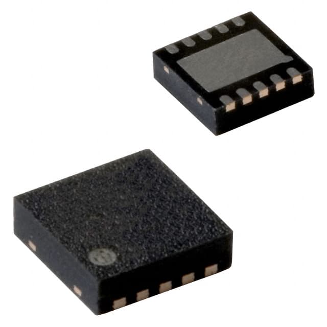
- Package: SOT23-6
- Essence: High-performance analog switch
- Packaging/Quantity: Tape and Reel, 3000 pieces per reel
Specifications
- Supply Voltage Range: 1.65V to 5.5V
- On-state Resistance: 2.5Ω (typical) at VCC = 3.3V
- On-state Resistance Flatness: 0.15Ω (typical)
- Bandwidth: 400MHz (-3dB)
- Crosstalk Rejection: -70dB at 10MHz
- Leakage Current: 1nA (typical) at TA = 25°C
- ESD Protection: ±8kV (HBM), ±200V (MM)
Detailed Pin Configuration
The NX3L4684TK,115 has a total of six pins arranged as follows: 1. Pin 1: IN1 (Input 1) 2. Pin 2: GND (Ground) 3. Pin 3: IN2 (Input 2) 4. Pin 4: VCC (Supply Voltage) 5. Pin 5: OUT (Output) 6. Pin 6: EN (Enable)
Functional Features
- Low voltage operation allows compatibility with various systems.
- Low power consumption ensures energy efficiency.
- High-speed switching enables fast signal routing.
- Wide bandwidth supports high-frequency applications.
- Excellent crosstalk rejection minimizes interference between channels.
Advantages and Disadvantages
Advantages: - Wide supply voltage range enhances versatility. - Low on-state resistance ensures minimal signal loss. - Compact SOT23-6 package saves board space. - High ESD protection safeguards against electrostatic discharge.
Disadvantages: - Limited number of channels (2 inputs and 1 output). - Not suitable for high-power applications.
Working Principles
The NX3L4684TK,115 is an analog switch that operates by controlling the connection between its input and output pins. When the EN pin is high, the switch is enabled, allowing the signal from either IN1 or IN2 to pass through to the OUT pin. Conversely, when the EN pin is low, the switch is disabled, and the IN and OUT pins are isolated.
Detailed Application Field Plans
The NX3L4684TK,115 finds applications in various fields, including: 1. Portable electronic devices: Enables signal routing in smartphones, tablets, and wearables. 2. Audio systems: Facilitates audio signal switching in headphones, speakers, and amplifiers. 3. Test and measurement equipment: Allows flexible signal routing in oscilloscopes, function generators, and data acquisition systems. 4. Industrial automation: Supports signal switching in control panels, PLCs, and sensors. 5. Automotive electronics: Enables signal routing in infotainment systems, navigation units, and vehicle diagnostics.
Detailed and Complete Alternative Models
- NX3L2467: Similar analog switch with 4 channels instead of 2.
- NX3L2267: Analog switch with 2 channels and lower on-state resistance.
- NX3L2267G: Analog switch with 2 channels and enhanced ESD protection.
(Note: The above alternative models are provided as examples and may not cover all available alternatives.)
This entry provides a comprehensive overview of the NX3L4684TK,115 analog switch, including its basic information, specifications, pin configuration, functional features, advantages, disadvantages, working principles, application field plans, and alternative models.
기술 솔루션에 NX3L4684TK,115 적용과 관련된 10가지 일반적인 질문과 답변을 나열하세요.
Sure! Here are 10 common questions and answers related to the application of NX3L4684TK,115:
1. What is the NX3L4684TK,115? The NX3L4684TK,115 is a high-performance, low-power, bidirectional voltage level translator with automatic direction sensing.
2. What is the operating voltage range of the NX3L4684TK,115? The operating voltage range of the NX3L4684TK,115 is from 1.65V to 5.5V.
3. How many channels does the NX3L4684TK,115 have? The NX3L4684TK,115 has four independent bidirectional channels.
4. What is the maximum data rate supported by the NX3L4684TK,115? The maximum data rate supported by the NX3L4684TK,115 is 100 Mbps.
5. Can the NX3L4684TK,115 be used for level shifting between different voltage domains? Yes, the NX3L4684TK,115 can be used for level shifting between different voltage domains, making it suitable for interfacing between devices with different logic levels.
6. Does the NX3L4684TK,115 require external pull-up or pull-down resistors? No, the NX3L4684TK,115 has built-in pull-up and pull-down resistors, eliminating the need for external components.
7. Is the NX3L4684TK,115 compatible with I2C and SPI interfaces? Yes, the NX3L4684TK,115 is compatible with both I2C and SPI interfaces, making it versatile for various applications.
8. Can the NX3L4684TK,115 handle bi-directional communication? Yes, the NX3L4684TK,115 supports bidirectional communication, allowing data to be transmitted in both directions.
9. What is the power supply voltage range for the NX3L4684TK,115? The power supply voltage range for the NX3L4684TK,115 is from 1.65V to 5.5V.
10. Is the NX3L4684TK,115 available in different package options? Yes, the NX3L4684TK,115 is available in different package options, including TSSOP and HVQFN, providing flexibility for different PCB layouts and space constraints.
Please note that these answers are general and may vary depending on the specific application and requirements. It's always recommended to refer to the datasheet and consult the manufacturer for detailed information.