

74LCX125BQX
Product Overview
Category
The 74LCX125BQX belongs to the category of integrated circuits (ICs) and specifically falls under the family of logic gates.
Use
This product is primarily used for signal level shifting and logic buffering in digital electronic circuits. It provides a convenient way to interface between devices operating at different voltage levels.
Characteristics
- Low-voltage operation: The 74LCX125BQX operates at a low voltage range, typically between 1.65V and 3.6V.
- High-speed performance: It offers fast switching speeds, making it suitable for high-frequency applications.
- Wide operating temperature range: The device can operate reliably within a wide temperature range, typically from -40°C to 85°C.
- Low power consumption: The 74LCX125BQX is designed to consume minimal power, making it energy-efficient.
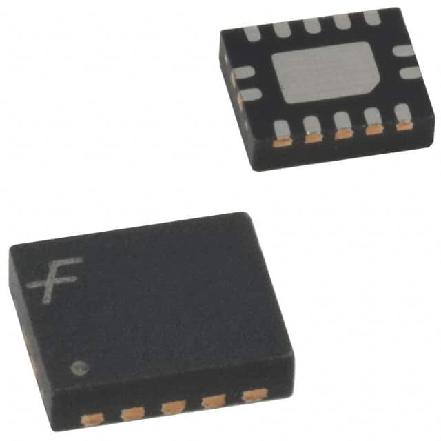
Package
The 74LCX125BQX is available in a small outline integrated circuit (SOIC) package. This package type provides ease of handling and compatibility with standard PCB manufacturing processes.
Essence
The essence of the 74LCX125BQX lies in its ability to provide voltage level translation and logic buffering functions, ensuring seamless communication between devices operating at different voltage levels.
Packaging/Quantity
The 74LCX125BQX is typically packaged in reels or tubes, containing a quantity of 250 or 300 units per package.
Specifications
- Supply Voltage Range: 1.65V to 3.6V
- Logic Family: LCX
- Number of Gates: 4
- Input/Output Compatibility: TTL/CMOS
- Propagation Delay: <5 ns
- Maximum Operating Frequency: 200 MHz
- Input Capacitance: 3 pF
- Output Drive Capability: ±24 mA
Detailed Pin Configuration
The 74LCX125BQX has a total of 14 pins, each serving a specific function. The pin configuration is as follows:
- GND (Ground)
- A1 (Input A1)
- Y1 (Output Y1)
- A2 (Input A2)
- Y2 (Output Y2)
- OE (Output Enable)
- Y3 (Output Y3)
- A3 (Input A3)
- VCC (Power Supply)
- Y4 (Output Y4)
- B1 (Input B1)
- B2 (Input B2)
- B3 (Input B3)
- GND (Ground)
Functional Features
- Voltage Level Shifting: The 74LCX125BQX allows for seamless translation of logic levels between different voltage domains, enabling compatibility between devices operating at varying voltages.
- Logic Buffering: It provides buffering capabilities to ensure signal integrity and prevent degradation when driving multiple loads or long traces.
- Output Enable Control: The OE pin allows the user to enable or disable the outputs, providing flexibility in controlling the flow of data.
Advantages and Disadvantages
Advantages
- Low-voltage operation makes it compatible with a wide range of digital systems.
- High-speed performance enables efficient data transmission in high-frequency applications.
- Low power consumption contributes to energy efficiency and longer battery life.
- Small package size facilitates space-saving integration into electronic designs.
Disadvantages
- Limited number of gates (4) may restrict its use in complex circuits requiring a higher gate count.
- Input/output compatibility limited to TTL/CMOS may not be suitable for all interface requirements.
Working Principles
The 74LCX125BQX operates based on complementary metal-oxide-semiconductor (CMOS) technology. It utilizes a combination of NMOS and PMOS transistors to achieve voltage level shifting and buffering functions. The inputs are protected against static discharge and excessive voltage levels, ensuring reliable operation.
Detailed Application Field Plans
The 74LCX125BQX finds applications in various fields, including but not limited to:
- Microcontrollers and microprocessors: It enables communication between devices operating at different voltage levels, facilitating seamless integration of peripherals.
- Communication systems: The device ensures compatibility between different logic families used in communication protocols, such as UART, SPI, and I2C.
- Industrial automation: It is utilized in control systems to interface between sensors, actuators, and programmable logic controllers (PLCs).
- Consumer electronics: The 74LCX125BQX is employed in devices like smartphones, tablets, and gaming consoles to enable efficient data transfer between components.
Detailed and Complete Alternative Models
Some alternative models that offer similar functionality to the 74LCX125BQX include:
- 74HCT125: This IC operates at higher voltage levels
기술 솔루션에 74LCX125BQX 적용과 관련된 10가지 일반적인 질문과 답변을 나열하세요.
Sure! Here are 10 common questions and answers related to the application of 74LCX125BQX in technical solutions:
Question: What is the 74LCX125BQX?
Answer: The 74LCX125BQX is a quad buffer gate with 3-state outputs, commonly used in digital logic circuits.Question: What is the maximum operating voltage for the 74LCX125BQX?
Answer: The maximum operating voltage for the 74LCX125BQX is 3.6V.Question: Can I use the 74LCX125BQX with a 5V power supply?
Answer: No, the 74LCX125BQX is not compatible with a 5V power supply. It is designed for lower voltage applications.Question: What is the output current capability of the 74LCX125BQX?
Answer: The 74LCX125BQX has a typical output current capability of ±24mA.Question: Can I connect multiple 74LCX125BQX devices together?
Answer: Yes, you can connect multiple 74LCX125BQX devices together to expand the number of buffer gates in your circuit.Question: Does the 74LCX125BQX have internal pull-up or pull-down resistors?
Answer: No, the 74LCX125BQX does not have internal pull-up or pull-down resistors. External resistors may be required if needed.Question: What is the propagation delay of the 74LCX125BQX?
Answer: The propagation delay of the 74LCX125BQX is typically around 3.5ns.Question: Can I use the 74LCX125BQX in high-speed applications?
Answer: Yes, the 74LCX125BQX is designed for high-speed operation and can be used in such applications.Question: Is the 74LCX125BQX compatible with both CMOS and TTL logic levels?
Answer: Yes, the 74LCX125BQX is compatible with both CMOS and TTL logic levels, making it versatile for various applications.Question: What is the package type of the 74LCX125BQX?
Answer: The 74LCX125BQX is available in a standard 14-pin TSSOP (Thin Shrink Small Outline Package) package.
Please note that these answers are general and may vary depending on the specific datasheet and manufacturer's specifications for the 74LCX125BQX.