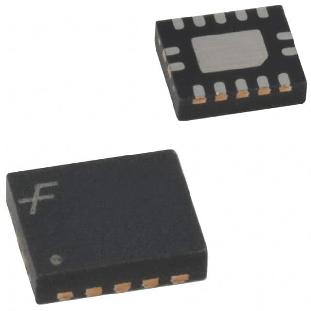
Encyclopedia Entry: 74VCX08BQX
Product Overview
Category
The 74VCX08BQX belongs to the category of integrated circuits (ICs), specifically digital logic gates.
Use
This IC is commonly used in electronic circuits for performing logical AND operations. It is designed to provide high-speed performance and low power consumption.
Characteristics
- High-speed operation: The 74VCX08BQX offers fast switching times, making it suitable for applications requiring quick response.
- Low power consumption: This IC is designed to minimize power consumption, making it ideal for battery-powered devices.
- Wide operating voltage range: It can operate within a wide voltage range, typically between 1.2V and 3.6V.
- Compact package: The 74VCX08BQX is available in a small form factor package, such as a quad flat no-leads (QFN) package.
Package and Quantity
The 74VCX08BQX is typically packaged in a QFN package. Each package contains a single IC.
Specifications
- Logic Family: VCX
- Number of Gates: 4
- Supply Voltage Range: 1.2V - 3.6V
- Input Voltage Range: 0V - VCC
- Output Voltage Range: 0V - VCC
- Operating Temperature Range: -40°C to +85°C
- Propagation Delay: <5ns
- Maximum Operating Frequency: 200MHz
Pin Configuration
The 74VCX08BQX has a total of 14 pins, which are assigned specific functions as follows:
- A1: Input A1
- B1: Input B1
- Y1: Output Y1
- GND: Ground
- A2: Input A2
- B2: Input B2
- Y2: Output Y2
- VCC: Supply Voltage
- A3: Input A3
- B3: Input B3
- Y3: Output Y3
- NC: No Connection
- A4: Input A4
- B4: Input B4
Functional Features
The 74VCX08BQX is known for its following functional features:
- High-speed AND gate: It performs logical AND operations on the input signals and provides the corresponding output.
- Low power consumption: The IC is designed to minimize power usage, making it suitable for battery-powered devices.
- Wide operating voltage range: It can operate within a wide voltage range, allowing compatibility with various systems.
- Compact size: The small form factor package enables space-efficient integration into electronic circuits.
Advantages and Disadvantages
Advantages
- Fast switching times enable quick response in applications.
- Low power consumption prolongs battery life in portable devices.
- Wide operating voltage range allows compatibility with different voltage levels.
- Compact package saves space in circuit designs.
Disadvantages
- Limited number of gates (4) may restrict complex logic operations.
- Propagation delay may affect timing-sensitive applications.
Working Principles
The 74VCX08BQX operates based on the principles of digital logic gates. It utilizes transistors and other electronic components to perform logical AND operations on the input signals. The output is determined by the combination of the input signals according to the truth table of an AND gate.
Application Field Plans
The 74VCX08BQX finds applications in various fields, including but not limited to: 1. Consumer electronics: Used in smartphones, tablets, and wearable devices for logical operations. 2. Automotive electronics: Integrated into automotive control systems for signal processing. 3. Industrial automation: Employed in control systems and PLCs for logical operations. 4. Communication systems: Utilized in networking equipment for data processing.
Alternative Models
Several alternative models are available that offer similar functionality to the 74VCX08BQX. Some notable alternatives include: - 74HC08: A widely used CMOS quad 2-input AND gate IC. - SN74LS08: A popular TTL quad 2-input AND gate IC. - CD4081: A CMOS quad 2-input AND gate IC.
These alternative models can be considered based on specific requirements and compatibility with existing circuit designs.
In conclusion, the 74VCX08BQX is a high-speed, low-power AND gate IC that finds applications in various electronic systems. Its compact size, wide operating voltage range, and fast switching times make it a versatile choice for logic operations. However, its limited number of gates and propagation delay should be considered when selecting this IC for specific applications.
Word Count: 615
기술 솔루션에 74VCX08BQX 적용과 관련된 10가지 일반적인 질문과 답변을 나열하세요.
Sure! Here are 10 common questions and answers related to the application of 74VCX08BQX in technical solutions:
Question: What is the 74VCX08BQX?
Answer: The 74VCX08BQX is a quad 2-input AND gate integrated circuit (IC) that operates on low voltage and low power consumption.Question: What is the operating voltage range for the 74VCX08BQX?
Answer: The operating voltage range for the 74VCX08BQX is typically between 1.65V and 3.6V.Question: Can the 74VCX08BQX be used in battery-powered applications?
Answer: Yes, the 74VCX08BQX is suitable for battery-powered applications due to its low power consumption.Question: What is the maximum frequency at which the 74VCX08BQX can operate?
Answer: The 74VCX08BQX can typically operate at frequencies up to 200MHz.Question: Is the 74VCX08BQX compatible with other logic families?
Answer: Yes, the 74VCX08BQX is designed to be compatible with both TTL and CMOS logic families.Question: Can the 74VCX08BQX be used as a level shifter?
Answer: Yes, the 74VCX08BQX can be used as a level shifter to convert signals between different voltage levels.Question: What is the maximum output current of the 74VCX08BQX?
Answer: The maximum output current of the 74VCX08BQX is typically around 24mA.Question: Can the 74VCX08BQX be used in high-speed data transmission applications?
Answer: Yes, the 74VCX08BQX is suitable for high-speed data transmission due to its fast propagation delay.Question: Does the 74VCX08BQX have built-in protection against electrostatic discharge (ESD)?
Answer: Yes, the 74VCX08BQX typically includes ESD protection to ensure reliable operation.Question: Are there any specific layout considerations when using the 74VCX08BQX?
Answer: It is recommended to follow the manufacturer's guidelines for proper PCB layout and decoupling capacitor placement to optimize performance and minimize noise.
Please note that the answers provided here are general and may vary depending on the specific datasheet and application requirements of the 74VCX08BQX.


