

7SB3257DTT1G
Product Overview
Category
The 7SB3257DTT1G belongs to the category of electronic components.
Use
This product is commonly used in electronic circuits for signal switching and routing purposes.
Characteristics
- High-speed switching capability
- Low power consumption
- Compact size
- Wide operating voltage range
Package
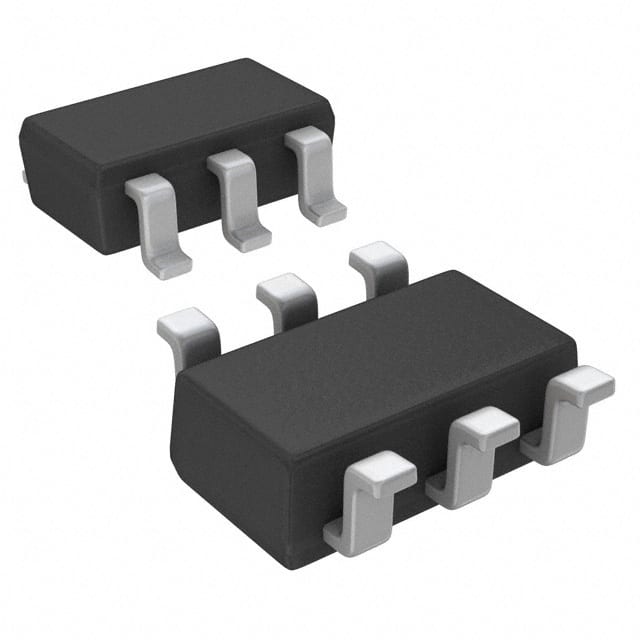
The 7SB3257DTT1G is typically available in a small surface-mount package, such as a Thin Small Outline Package (TSOP) or a Quad Flat No-Lead (QFN) package.
Essence
The essence of the 7SB3257DTT1G lies in its ability to provide efficient signal switching and routing functionality within electronic circuits.
Packaging/Quantity
This product is usually packaged in reels or trays, with quantities varying depending on the manufacturer's specifications. Typical quantities range from a few hundred to several thousand units per package.
Specifications
- Supply Voltage: 2.0V - 5.5V
- On-state resistance: 4Ω (typical)
- Maximum Input Voltage: VCC + 0.5V
- Maximum Output Current: ±32mA
- Operating Temperature Range: -40°C to +85°C
Detailed Pin Configuration
The 7SB3257DTT1G consists of eight pins, each serving a specific function:
- Pin 1: Enable (EN)
- Pin 2: Channel 1 Data Input/Output (A1)
- Pin 3: Channel 2 Data Input/Output (B1)
- Pin 4: Channel 3 Data Input/Output (A2)
- Pin 5: Channel 4 Data Input/Output (B2)
- Pin 6: Channel 1 Enable (OE1)
- Pin 7: Channel 2 Enable (OE2)
- Pin 8: Ground (GND)
Functional Features
- Quad bilateral switch with independent enable control
- Low ON-state resistance for minimal signal distortion
- Wide operating voltage range allows compatibility with various systems
- Fast switching speed for efficient signal routing
Advantages and Disadvantages
Advantages
- High-speed switching capability enables efficient signal routing in electronic circuits.
- Low power consumption contributes to energy efficiency.
- Compact size allows for space-saving integration into circuit designs.
- Wide operating voltage range ensures compatibility with different systems.
Disadvantages
- Limited maximum output current may restrict usage in high-power applications.
- The need for external enable control may add complexity to circuit design.
Working Principles
The 7SB3257DTT1G operates based on the principles of solid-state switching. When the enable pin is activated, the corresponding channel's data input/output pins are connected, allowing the signal to pass through. Conversely, when the enable pin is deactivated, the channels are isolated, preventing signal transmission.
Detailed Application Field Plans
The 7SB3257DTT1G finds application in various fields, including but not limited to: - Audio and video equipment - Telecommunications devices - Computer peripherals - Industrial automation systems - Automotive electronics
Detailed and Complete Alternative Models
Some alternative models that offer similar functionality to the 7SB3257DTT1G include: - SN74CBT3257C - CD74HC4053 - DG406DJ
These alternatives can be considered based on specific requirements and compatibility with the target system.
In conclusion, the 7SB3257DTT1G is a versatile electronic component that provides efficient signal switching and routing capabilities. Its compact size, low power consumption, and wide operating voltage range make it suitable for various applications in different industries. However, its limited maximum output current and the need for external enable control should be taken into consideration during circuit design.
기술 솔루션에 7SB3257DTT1G 적용과 관련된 10가지 일반적인 질문과 답변을 나열하세요.
Sure! Here are 10 common questions and answers related to the application of 7SB3257DTT1G in technical solutions:
Q1: What is the 7SB3257DTT1G? A1: The 7SB3257DTT1G is a multiplexer/demultiplexer switch IC (integrated circuit) that allows for bidirectional signal switching between two ports.
Q2: What is the voltage rating of the 7SB3257DTT1G? A2: The 7SB3257DTT1G has a voltage rating of up to 5.5V.
Q3: How many channels does the 7SB3257DTT1G have? A3: The 7SB3257DTT1G has four independent channels, allowing for simultaneous switching of multiple signals.
Q4: What is the maximum current handling capability of the 7SB3257DTT1G? A4: The 7SB3257DTT1G can handle a maximum continuous current of 500mA per channel.
Q5: Can the 7SB3257DTT1G be used for analog signals? A5: Yes, the 7SB3257DTT1G can be used for both digital and analog signals.
Q6: What is the typical on-resistance of the 7SB3257DTT1G? A6: The typical on-resistance of the 7SB3257DTT1G is around 4 ohms.
Q7: Is the 7SB3257DTT1G compatible with different logic families? A7: Yes, the 7SB3257DTT1G is compatible with various logic families such as TTL, CMOS, and LVCMOS.
Q8: Can the 7SB3257DTT1G be used in high-speed applications? A8: Yes, the 7SB3257DTT1G is suitable for high-speed applications with a typical propagation delay of around 5ns.
Q9: Does the 7SB3257DTT1G have built-in ESD protection? A9: Yes, the 7SB3257DTT1G has built-in ESD (electrostatic discharge) protection to safeguard against damage during handling and operation.
Q10: What package options are available for the 7SB3257DTT1G? A10: The 7SB3257DTT1G is available in various package options, including SOT-363 and SC-88A.
Please note that these answers are general and may vary depending on the specific datasheet and manufacturer's specifications for the 7SB3257DTT1G.