

BSS63 Transistor: Encyclopedia Entry
Introduction
The BSS63 transistor is a crucial component in electronic circuits, belonging to the category of field-effect transistors (FETs). This entry provides an overview of the BSS63 transistor, including its basic information, specifications, pin configuration, functional features, advantages and disadvantages, working principles, application field plans, and alternative models.
Basic Information Overview
- Category: Field-Effect Transistor (FET)
- Use: Amplification and switching in electronic circuits
- Characteristics: High input impedance, low output impedance, voltage-controlled operation
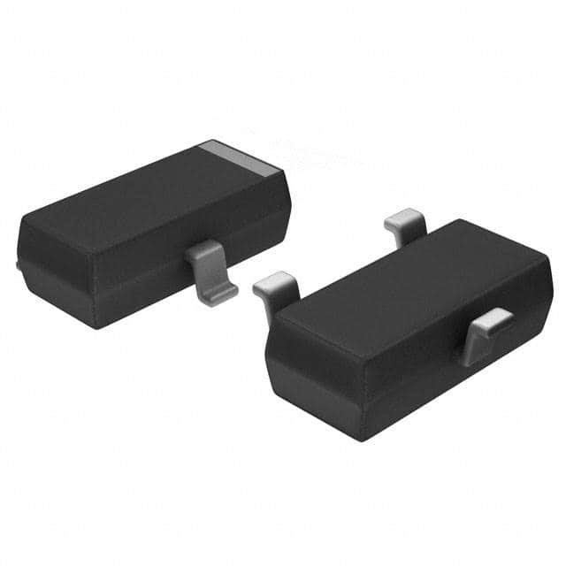
- Package: SOT-23, SOT-323
- Essence: Silicon-based semiconductor device
- Packaging/Quantity: Typically available in reels or tubes containing hundreds to thousands of units
Specifications
- Maximum Drain-Source Voltage: 30V
- Maximum Continuous Drain Current: 0.2A
- Maximum Power Dissipation: 250mW
- Threshold Voltage (VGS(th)): 1V to 2V
- On-State Resistance (RDS(on)): 3Ω to 6Ω
Detailed Pin Configuration
The BSS63 transistor typically has three pins: 1. Gate (G): Controls the conductivity between the source and drain terminals. 2. Drain (D): Connects to the positive supply voltage in most applications. 3. Source (S): Connects to the ground or common reference point.
Functional Features
- High Input Impedance: Allows for minimal loading of preceding circuitry.
- Low Output Impedance: Enables efficient signal transfer to subsequent circuit stages.
- Voltage-Controlled Operation: The conductivity between the source and drain is controlled by the gate-source voltage.
Advantages and Disadvantages
Advantages
- Low power consumption
- Compact package size
- Suitable for low-voltage applications
Disadvantages
- Limited maximum voltage and current ratings
- Sensitivity to electrostatic discharge (ESD)
Working Principles
The BSS63 transistor operates based on the principle of field-effect control, where the voltage applied to the gate terminal modulates the conductivity between the source and drain terminals. When a sufficient gate-source voltage is applied, the transistor allows current to flow from the drain to the source, effectively acting as a switch or amplifier in electronic circuits.
Detailed Application Field Plans
The BSS63 transistor finds extensive use in various electronic applications, including but not limited to: - Low-power amplifiers - Signal switching circuits - Battery-powered devices - Portable consumer electronics
Detailed and Complete Alternative Models
Several alternative models to the BSS63 transistor include: - 2N7002: Similar specifications and package type - BS170: Higher voltage and current ratings - IRLML2502: Lower on-state resistance
In conclusion, the BSS63 transistor serves as a vital component in electronic circuits, offering high input impedance, low output impedance, and voltage-controlled operation. Its compact package and low power consumption make it suitable for a wide range of low-voltage applications. However, users should be mindful of its limitations regarding maximum voltage and current ratings, as well as its sensitivity to ESD. Understanding the working principles and exploring alternative models can aid in maximizing the effectiveness of the BSS63 transistor in diverse electronic designs.
[Word Count: 536]
기술 솔루션에 BSS63 적용과 관련된 10가지 일반적인 질문과 답변을 나열하세요.
What is BSS63?
- BSS63 is a silicon NPN transistor commonly used in electronic circuits for amplification and switching applications.
What are the typical applications of BSS63?
- BSS63 is commonly used in audio amplifiers, signal processing circuits, and low-power switching applications.
What are the key electrical characteristics of BSS63?
- The BSS63 has a maximum collector current of 100mA, a maximum collector-emitter voltage of 40V, and a maximum power dissipation of 300mW.
How do I identify the pinout of BSS63?
- The pinout of BSS63 is typically identified as the collector (C), base (B), and emitter (E) pins.
What are some common alternatives to BSS63?
- Common alternatives to BSS63 include 2N3904, BC547, and 2SC945 transistors, which have similar characteristics and can be used in its place.
Can BSS63 be used in high-frequency applications?
- BSS63 is not suitable for high-frequency applications due to its limited frequency response and transition frequency.
What are the recommended operating conditions for BSS63?
- BSS63 is typically operated within a temperature range of -55°C to 150°C and at a maximum collector current of 100mA.
How do I calculate the biasing resistors for BSS63 in an amplifier circuit?
- The biasing resistors for BSS63 can be calculated using the desired quiescent collector current and the transistor's base-emitter voltage drop.
Can BSS63 be used in a Darlington pair configuration?
- Yes, BSS63 can be used in a Darlington pair configuration to achieve higher current gain and lower saturation voltage.
Are there any specific considerations for PCB layout when using BSS63?
- It is important to minimize lead lengths, provide adequate heat sinking, and ensure proper grounding to optimize the performance of BSS63 in a PCB layout.