

DTC143ZET1G
Introduction
The DTC143ZET1G is a bipolar junction transistor (BJT) belonging to the category of discrete semiconductor devices. This device is commonly used in electronic circuits for amplification and switching applications due to its unique characteristics and performance.
Basic Information Overview
- Category: Discrete Semiconductor Device
- Use: Amplification and Switching in Electronic Circuits
- Characteristics: High Gain, Low Noise, Small Package Size
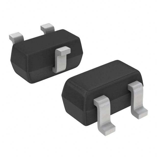
- Package: SOT-23-3
- Essence: NPN Bipolar Junction Transistor
- Packaging/Quantity: Tape & Reel, 3000 units per reel
Specifications
- Collector-Base Voltage (VCBO): 50V
- Collector-Emitter Voltage (VCEO): 50V
- Emitter-Base Voltage (VEBO): 5V
- Collector Current (IC): 100mA
- Power Dissipation (PD): 225mW
- Transition Frequency (fT): 250MHz
- Operating Temperature Range: -55°C to 150°C
Detailed Pin Configuration
The DTC143ZET1G has three pins: 1. Emitter (E) 2. Base (B) 3. Collector (C)
Functional Features
- High current gain (hFE)
- Low noise
- Fast switching speed
- Small package size for space-constrained designs
Advantages and Disadvantages
Advantages
- High gain allows for signal amplification
- Low noise makes it suitable for sensitive applications
- Small package size enables compact circuit design
Disadvantages
- Limited collector current compared to power transistors
- Limited power dissipation capability
Working Principles
The DTC143ZET1G operates based on the principles of bipolar junction transistors. When a small current flows into the base terminal, it controls a larger current flow between the collector and emitter terminals, allowing for amplification or switching of signals in electronic circuits.
Detailed Application Field Plans
The DTC143ZET1G is widely used in various electronic applications, including: - Audio amplifiers - Signal processing circuits - Switching circuits - Sensor interfaces - Oscillator circuits
Detailed and Complete Alternative Models
Some alternative models to the DTC143ZET1G include: - BC547B - 2N3904 - 2SC945 - KSP2222A
In conclusion, the DTC143ZET1G is a versatile NPN bipolar junction transistor with high gain and low noise characteristics, making it suitable for a wide range of amplification and switching applications in electronic circuits.
[Word Count: 320]
기술 솔루션에 DTC143ZET1G 적용과 관련된 10가지 일반적인 질문과 답변을 나열하세요.
What is the maximum collector current of DTC143ZET1G?
- The maximum collector current of DTC143ZET1G is 100mA.
What is the typical hFE (DC current gain) of DTC143ZET1G?
- The typical hFE of DTC143ZET1G is 120-400 at VCE = 5V, IC = 2mA.
What is the maximum VCE (collector-emitter voltage) of DTC143ZET1G?
- The maximum VCE of DTC143ZET1G is 50V.
What are the package dimensions of DTC143ZET1G?
- DTC143ZET1G comes in a SOT-323 package with dimensions of 2.00mm x 1.25mm x 1.10mm.
What is the power dissipation of DTC143ZET1G?
- The power dissipation of DTC143ZET1G is 150mW.
What are the recommended operating and storage temperatures for DTC143ZET1G?
- The recommended operating temperature range for DTC143ZET1G is -55°C to 150°C, and the storage temperature range is -55°C to 150°C.
Is DTC143ZET1G RoHS compliant?
- Yes, DTC143ZET1G is RoHS compliant.
What are the typical applications of DTC143ZET1G?
- DTC143ZET1G is commonly used in switching and amplification applications in various electronic circuits.
Does DTC143ZET1G require external base resistor for operation?
- Yes, DTC143ZET1G requires an external base resistor for proper operation.
What are the key differences between DTC143ZET1G and similar transistors?
- DTC143ZET1G offers low saturation voltage and high current gain compared to similar transistors, making it suitable for specific technical solutions.