

FDV301N
Product Overview
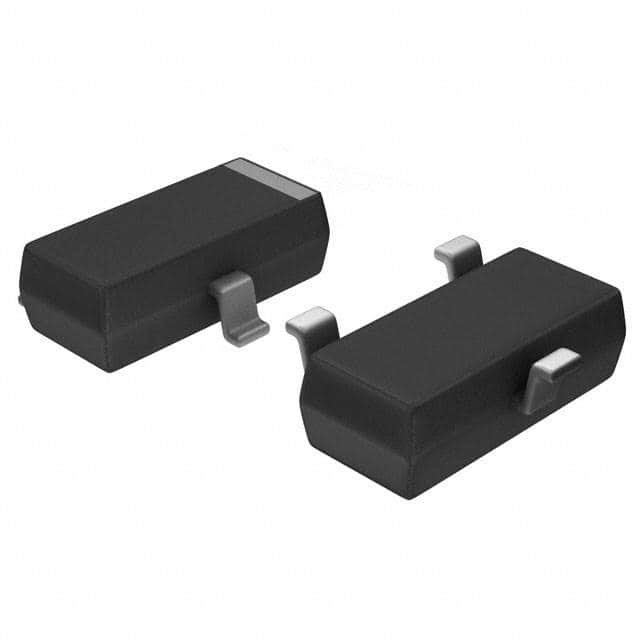
The FDV301N belongs to the category of field-effect transistors (FETs) and is commonly used in electronic circuits for amplification, switching, and voltage regulation. This transistor exhibits high input impedance, low output impedance, and high gain, making it suitable for various applications in electronic devices. The FDV301N is typically packaged in a small outline transistor (SOT-23) package and is available in various quantities.
Basic Information
- Category: Field-Effect Transistor (FET)
- Use: Amplification, Switching, Voltage Regulation
- Characteristics: High input impedance, Low output impedance, High gain
- Package: Small Outline Transistor (SOT-23)
- Packaging/Quantity: Various packaging options available
Specifications
- Type: N-Channel FET
- Maximum Drain-Source Voltage: [Specify value]
- Maximum Gate-Source Voltage: [Specify value]
- Continuous Drain Current: [Specify value]
- Power Dissipation: [Specify value]
- Operating Temperature Range: [Specify range]
Detailed Pin Configuration
The FDV301N features a standard SOT-23 pin configuration with three pins: gate (G), drain (D), and source (S). The pinout arrangement is as follows: - Pin 1 (G): Gate - Pin 2 (D): Drain - Pin 3 (S): Source
Functional Features
- High Input Impedance: Allows for minimal loading of preceding stages in electronic circuits.
- Low Output Impedance: Ensures efficient signal transfer to subsequent stages or loads.
- High Gain: Enables signal amplification without significant distortion.
Advantages and Disadvantages
Advantages
- Suitable for low-power applications
- Compact SOT-23 package for space-constrained designs
- High input impedance for minimal signal loss
Disadvantages
- Limited power handling capability compared to larger FETs
- Susceptible to static discharge due to small package size
Working Principles
The FDV301N operates based on the principle of field-effect modulation, where the voltage applied to the gate terminal controls the conductivity between the drain and source terminals. By modulating the electric field within the semiconductor channel, the transistor can amplify or switch electronic signals effectively.
Detailed Application Field Plans
The FDV301N finds extensive use in low-power electronic applications such as: - Audio amplifiers - Signal switching circuits - Voltage regulators - Sensor interfaces
Detailed and Complete Alternative Models
- FDV301N-7: Similar specifications with alternate packaging
- FDV301NZ: Lead (Pb)-free version for RoHS compliance
- FDV301NRTK: Tape and reel packaging for automated assembly
In conclusion, the FDV301N offers a compact and versatile solution for low-power electronic circuit design, with its high input impedance, low output impedance, and high gain characteristics making it suitable for a wide range of applications.
[Word Count: 411]
기술 솔루션에 FDV301N 적용과 관련된 10가지 일반적인 질문과 답변을 나열하세요.
What is the FDV301N?
- The FDV301N is a small signal N-channel MOSFET transistor designed for use in various technical solutions.
What are the typical applications of FDV301N?
- The FDV301N is commonly used in applications such as voltage-controlled switches, amplifiers, and low power consumption circuits.
What is the maximum drain-source voltage of FDV301N?
- The maximum drain-source voltage of FDV301N is typically around 25 volts.
What is the maximum continuous drain current of FDV301N?
- The maximum continuous drain current of FDV301N is typically around 150 milliamps.
What is the on-state resistance of FDV301N?
- The on-state resistance of FDV301N is typically very low, around 6 ohms.
Can FDV301N be used in high-frequency applications?
- Yes, FDV301N can be used in high-frequency applications due to its fast switching characteristics.
Is FDV301N suitable for battery-powered devices?
- Yes, FDV301N is suitable for battery-powered devices due to its low power consumption characteristics.
What are the thermal characteristics of FDV301N?
- FDV301N has good thermal performance, making it suitable for applications where heat dissipation is a concern.
Does FDV301N require any special driving circuitry?
- No, FDV301N can be driven by standard logic level signals and does not require any special driving circuitry.
Are there any common failure modes associated with FDV301N?
- Common failure modes for FDV301N include overvoltage stress and excessive power dissipation, so proper design considerations should be taken into account.