

NSVBC847BLT3G
Introduction
The NSVBC847BLT3G is a versatile semiconductor component that belongs to the category of voltage level shifters. This device is commonly used in electronic circuits to convert logic levels between different voltage domains, making it an essential component in various applications.
Basic Information Overview
- Category: Voltage Level Shifter
- Use: Logic level conversion between different voltage domains
- Characteristics: Fast switching speed, low power consumption, compact size
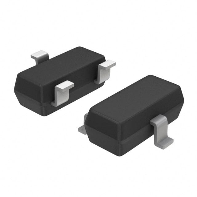
- Package: SOT-23-5 package
- Essence: Facilitates seamless integration of components operating at different voltage levels
- Packaging/Quantity: Typically available in reels of 3000 units
Specifications
- Input Voltage Range: 0.8V to 5.5V
- Output Voltage Range: -0.5V to 5.5V
- Operating Temperature Range: -40°C to 125°C
- Maximum Propagation Delay: 10ns
- Supply Voltage: 1.65V to 5.5V
- Quiescent Current: 1µA
Detailed Pin Configuration
The NSVBC847BLT3G typically features the following pin configuration: 1. VCCA (Input Voltage A) 2. VCCB (Input Voltage B) 3. A1 (Channel A Input) 4. A2 (Channel A Output) 5. GND (Ground)
Functional Features
- Bi-directional level shifting
- High-speed operation
- Low power consumption
- ESD protection
- Small form factor
Advantages and Disadvantages
Advantages
- Seamless integration of components with different voltage requirements
- Fast switching speed
- Low power consumption
- Compact size
Disadvantages
- Limited current handling capacity
- Sensitivity to voltage spikes
Working Principles
The NSVBC847BLT3G operates by utilizing internal circuitry to translate input logic levels from one voltage domain to another. It employs MOSFET-based level shifting techniques to ensure efficient and reliable signal translation.
Detailed Application Field Plans
The NSVBC847BLT3G finds extensive application in various electronic systems, including: - Battery management systems - Portable consumer electronics - Industrial automation - IoT devices - Communication equipment
Detailed and Complete Alternative Models
Some alternative models to the NSVBC847BLT3G include: - TXS0102DCTR: Dual-Bit Bidirectional Voltage-Level Translator - SN74LVC1T45DBVR: Single-Bit Dual-Supply Bus Transceiver - PCA9306DCUR: Dual Bidirectional I2C-Bus and SMBus Voltage-Level Translator
In conclusion, the NSVBC847BLT3G serves as a crucial component in modern electronic systems, enabling seamless integration of components operating at different voltage levels while offering fast switching speeds and low power consumption.
Word Count: 398
기술 솔루션에 NSVBC847BLT3G 적용과 관련된 10가지 일반적인 질문과 답변을 나열하세요.
What is NSVBC847BLT3G?
- NSVBC847BLT3G is a high-performance, low VCE(sat) NPN bipolar transistor in a small SOT-23 package, commonly used in various technical solutions.
What are the key features of NSVBC847BLT3G?
- The key features of NSVBC847BLT3G include low VCE(sat), high current gain, and a small form factor, making it suitable for space-constrained applications.
In what technical solutions is NSVBC847BLT3G commonly used?
- NSVBC847BLT3G is commonly used in applications such as voltage regulators, power management circuits, and general amplification circuits.
What are the typical operating conditions for NSVBC847BLT3G?
- The typical operating conditions for NSVBC847BLT3G include a maximum collector current (IC) of 100mA, a maximum collector-emitter voltage (VCEO) of 50V, and a maximum power dissipation of 225mW.
How does NSVBC847BLT3G compare to other transistors in its class?
- NSVBC847BLT3G offers lower VCE(sat) and higher current gain compared to many other transistors in its class, making it suitable for high-efficiency applications.
Can NSVBC847BLT3G be used in switching applications?
- Yes, NSVBC847BLT3G can be used in low-power switching applications due to its low VCE(sat) and fast switching characteristics.
What are the recommended thermal considerations for NSVBC847BLT3G?
- It is recommended to use proper heat sinking and thermal management techniques when designing with NSVBC847BLT3G to ensure optimal performance and reliability.
Are there any specific layout considerations when using NSVBC847BLT3G in a circuit?
- It is important to minimize trace lengths and optimize PCB layout to reduce parasitic effects and ensure stable operation of NSVBC847BLT3G.
What are the potential failure modes of NSVBC847BLT3G?
- Potential failure modes of NSVBC847BLT3G include overcurrent, overvoltage, and excessive junction temperature, which can lead to degradation or permanent damage.
Where can I find detailed application notes and design guidelines for NSVBC847BLT3G?
- Detailed application notes and design guidelines for NSVBC847BLT3G can be found in the product datasheet, as well as on the manufacturer's website and technical literature.