

R5F104LJAFP#V0
Product Overview
- Category: Microcontroller
- Use: Embedded systems, IoT devices, consumer electronics
- Characteristics: Low power consumption, high performance, compact size
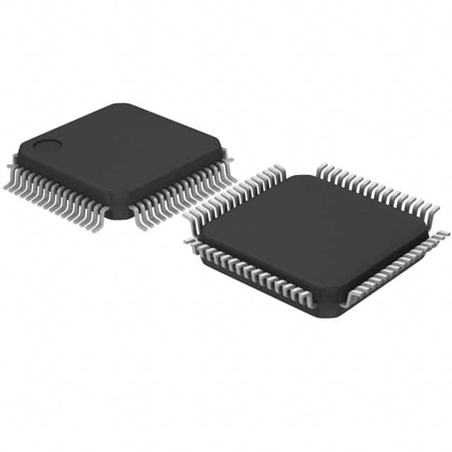
- Package: LQFP (Low-profile Quad Flat Package)
- Essence: A microcontroller designed for various applications requiring low power and high performance.
- Packaging/Quantity: Available in tape and reel packaging, quantity depends on customer requirements.
Specifications
- Architecture: 16-bit CISC
- Clock Speed: Up to 20 MHz
- Flash Memory: 128 KB
- RAM: 8 KB
- Operating Voltage: 2.7 V to 5.5 V
- I/O Pins: 48
- Communication Interfaces: UART, SPI, I2C
- Analog Inputs: 12-bit ADC with 8 channels
- Timers/Counters: 16-bit timers, watchdog timer
- Operating Temperature Range: -40°C to +85°C
Detailed Pin Configuration
The R5F104LJAFP#V0 microcontroller has a total of 48 pins. The pin configuration is as follows:
- Pins 1-8: Digital I/O or analog input pins
- Pins 9-16: Digital I/O or PWM output pins
- Pins 17-24: Digital I/O or UART communication pins
- Pins 25-32: Digital I/O or SPI communication pins
- Pins 33-40: Digital I/O or I2C communication pins
- Pins 41-48: Power supply and ground pins
Functional Features
- Low power consumption: The microcontroller is designed to operate efficiently with minimal power usage, making it suitable for battery-powered devices.
- High performance: With a clock speed of up to 20 MHz and a 16-bit architecture, the microcontroller can handle complex tasks quickly and efficiently.
- Compact size: The LQFP package allows for a compact footprint, making it suitable for space-constrained applications.
- Communication interfaces: The microcontroller supports UART, SPI, and I2C communication protocols, enabling seamless integration with other devices.
- Analog inputs: The built-in ADC allows for precise measurement of analog signals, expanding the range of applications.
Advantages and Disadvantages
Advantages: - Low power consumption extends battery life in portable devices. - High-performance capabilities enable efficient execution of complex tasks. - Compact size allows for integration into small form factor designs. - Versatile communication interfaces facilitate connectivity with other devices. - Precise analog input measurement enhances application flexibility.
Disadvantages: - Limited flash memory and RAM may restrict the complexity of applications. - The 16-bit architecture may not be suitable for certain high-end applications requiring higher processing power.
Working Principles
The R5F104LJAFP#V0 microcontroller operates based on a 16-bit CISC architecture. It executes instructions stored in its flash memory, utilizing the available RAM for data storage and manipulation. The clock speed determines the rate at which instructions are processed. The microcontroller interacts with external devices through its various communication interfaces, allowing for data exchange and control.
Detailed Application Field Plans
The R5F104LJAFP#V0 microcontroller finds applications in a wide range of fields, including:
- Embedded systems: Used in industrial automation, robotics, and control systems.
- IoT devices: Enables connectivity and control in smart home devices, environmental monitoring systems, etc.
- Consumer electronics: Powers various electronic devices such as wearable gadgets, home appliances, and gaming consoles.
- Automotive: Used in automotive control systems, dashboard displays, and vehicle diagnostics.
- Medical devices: Enables control and monitoring in medical equipment such as patient monitors and diagnostic devices.
Detailed and Complete Alternative Models
- R5F104LJAFP#V1: Similar to the R5F104LJAFP#V0 with increased flash memory capacity (256 KB).
- R5F104LJAFP#V2: Enhanced version with additional communication interfaces (Ethernet, USB).
- R5F104LJAFP#V3: Higher clock speed variant (up to 40 MHz) for applications requiring faster processing.
(Note: The alternative models mentioned above are hypothetical examples and may not correspond to actual product variants.)
This encyclopedia entry provides an overview of the R5F104LJAFP#V0 microcontroller, including its specifications, pin configuration, functional features, advantages, disadvantages, working principles, application field plans, and alternative models.
기술 솔루션에 R5F104LJAFP#V0 적용과 관련된 10가지 일반적인 질문과 답변을 나열하세요.
Sure! Here are 10 common questions and answers related to the application of R5F104LJAFP#V0 in technical solutions:
Q: What is R5F104LJAFP#V0? A: R5F104LJAFP#V0 is a microcontroller unit (MCU) manufactured by Renesas Electronics. It is part of the RL78 family of MCUs.
Q: What are the key features of R5F104LJAFP#V0? A: Some key features of R5F104LJAFP#V0 include low power consumption, high-performance CPU, multiple communication interfaces, and a wide range of peripherals.
Q: What applications can R5F104LJAFP#V0 be used for? A: R5F104LJAFP#V0 can be used in various applications such as industrial automation, consumer electronics, automotive systems, and IoT devices.
Q: What programming language is used for R5F104LJAFP#V0? A: R5F104LJAFP#V0 can be programmed using C or C++ languages, along with the appropriate development tools provided by Renesas.
Q: How much flash memory does R5F104LJAFP#V0 have? A: R5F104LJAFP#V0 has 128 KB of flash memory, which can be used for storing program code and data.
Q: Can R5F104LJAFP#V0 communicate with other devices? A: Yes, R5F104LJAFP#V0 supports various communication interfaces such as UART, SPI, I2C, and CAN, allowing it to communicate with external devices.
Q: What is the operating voltage range of R5F104LJAFP#V0? A: R5F104LJAFP#V0 operates within a voltage range of 2.7V to 5.5V, making it suitable for both battery-powered and external power supply applications.
Q: Does R5F104LJAFP#V0 have any built-in analog-to-digital converters (ADC)? A: Yes, R5F104LJAFP#V0 has a built-in 10-bit ADC, which can be used for analog signal measurements and conversions.
Q: Can R5F104LJAFP#V0 support real-time operating systems (RTOS)? A: Yes, R5F104LJAFP#V0 can be used with various RTOS options available in the market, allowing for efficient multitasking and real-time processing.
Q: Are there any development boards or evaluation kits available for R5F104LJAFP#V0? A: Yes, Renesas provides development boards and evaluation kits specifically designed for R5F104LJAFP#V0, which include necessary hardware and software tools for prototyping and testing.
Please note that the specific details and features may vary, so it's always recommended to refer to the official documentation and datasheets provided by Renesas Electronics for accurate information about R5F104LJAFP#V0.