

BR24T16FV-WE2
Introduction
The BR24T16FV-WE2 is a versatile and advanced product that belongs to the category of non-volatile memory devices. This entry provides an overview of its basic information, specifications, detailed pin configuration, functional features, advantages and disadvantages, working principles, detailed application field plans, and alternative models.
Basic Information Overview
- Category: Non-volatile Memory Device
- Use: Data storage and retrieval in electronic systems
- Characteristics: High-speed read and write operations, low power consumption, compact form factor
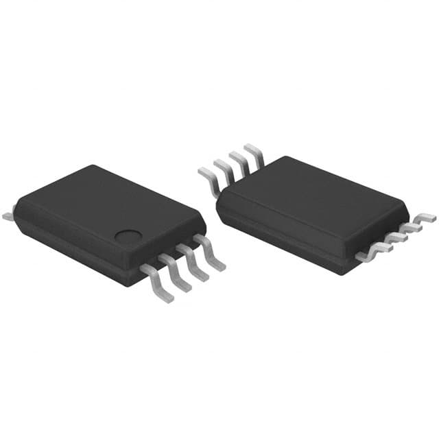
- Package: Small outline package (SOP)
- Essence: Reliable and efficient data storage solution
- Packaging/Quantity: Available in tape and reel packaging with varying quantities
Specifications
- Capacity: 16 kilobits (2 Kbytes)
- Interface: I2C (Inter-Integrated Circuit) compatible
- Operating Voltage: 1.7V to 5.5V
- Operating Temperature: -40°C to 85°C
- Data Retention: Minimum of 200 years
- Write Endurance: Minimum of 1 million cycles
Detailed Pin Configuration
The BR24T16FV-WE2 features a standard 8-pin SOP package with the following pin configuration: 1. VCC (Power Supply) 2. GND (Ground) 3. SDA (Serial Data) 4. SCL (Serial Clock) 5. WP (Write Protect) 6. NC (No Connection) 7. A0 (Chip Address Input) 8. A1 (Chip Address Input)
Functional Features
- High-Speed Operation: Enables quick data access and transfer
- Low Power Consumption: Ideal for battery-powered applications
- Write Protection: Ensures data integrity by preventing accidental writes
- I2C Compatibility: Allows easy integration into various systems
- Reliability: Long data retention and high write endurance
Advantages and Disadvantages
Advantages
- Fast read and write operations
- Low power consumption
- Enhanced data security with write protection
- Wide operating voltage range
- Compact form factor
Disadvantages
- Limited capacity compared to larger memory devices
- Higher cost per bit compared to bulk memory solutions
Working Principles
The BR24T16FV-WE2 utilizes non-volatile memory technology to store and retrieve data. It employs the I2C interface for communication with the host system, allowing seamless integration and data transfer. The device's internal architecture ensures reliable and efficient operation while maintaining low power consumption.
Detailed Application Field Plans
The BR24T16FV-WE2 is well-suited for a wide range of applications, including but not limited to: - Consumer electronics - Industrial automation - Automotive systems - Medical devices - IoT (Internet of Things) devices
Detailed and Complete Alternative Models
- BR24T08FV-WE2: 8 kilobit (1 Kbyte) capacity variant
- BR24T32FV-WE2: 32 kilobit (4 Kbyte) capacity variant
- BR24T64FV-WE2: 64 kilobit (8 Kbyte) capacity variant
In conclusion, the BR24T16FV-WE2 offers a reliable and efficient non-volatile memory solution with high-speed operation, low power consumption, and enhanced data security features. Its versatility makes it suitable for a wide range of applications across various industries.
Word count: 443
기술 솔루션에 BR24T16FV-WE2 적용과 관련된 10가지 일반적인 질문과 답변을 나열하세요.
What is the maximum operating temperature of BR24T16FV-WE2?
- The maximum operating temperature of BR24T16FV-WE2 is 85°C.
What is the typical voltage supply range for BR24T16FV-WE2?
- The typical voltage supply range for BR24T16FV-WE2 is 1.7V to 5.5V.
What is the data retention period for BR24T16FV-WE2?
- The data retention period for BR24T16FV-WE2 is 100 years.
Does BR24T16FV-WE2 support I2C communication?
- Yes, BR24T16FV-WE2 supports I2C communication.
What is the typical standby current consumption of BR24T16FV-WE2?
- The typical standby current consumption of BR24T16FV-WE2 is 1μA.
Is BR24T16FV-WE2 compatible with industrial temperature ranges?
- Yes, BR24T16FV-WE2 is compatible with industrial temperature ranges.
What is the maximum clock frequency supported by BR24T16FV-WE2?
- The maximum clock frequency supported by BR24T16FV-WE2 is 400kHz.
Does BR24T16FV-WE2 have built-in write protection features?
- Yes, BR24T16FV-WE2 has built-in write protection features.
What is the package type of BR24T16FV-WE2?
- BR24T16FV-WE2 comes in a SOP-8 package.
Can BR24T16FV-WE2 be used in automotive applications?
- Yes, BR24T16FV-WE2 can be used in automotive applications as it is AEC-Q100 qualified.