

STP100N10F7
Product Overview
Category
The STP100N10F7 belongs to the category of power MOSFETs.
Use
It is used as a high-voltage, fast-switching N-channel enhancement-mode power MOSFET.
Characteristics
- High voltage capability
- Low input capacitance
- Fast switching speed
- Low on-resistance
Package
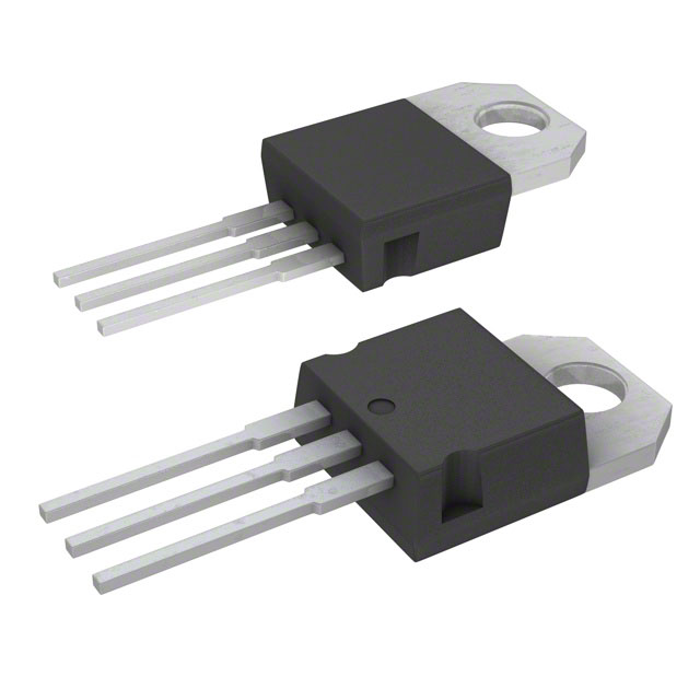
The STP100N10F7 is typically available in a TO-220 package.
Essence
The essence of the STP100N10F7 lies in its ability to efficiently control high voltages and currents in various electronic applications.
Packaging/Quantity
It is commonly packaged in reels or tubes, with quantities varying based on manufacturer specifications.
Specifications
- Drain-Source Voltage (VDS): 100V
- Continuous Drain Current (ID): 100A
- On-Resistance (RDS(on)): 0.007 ohms
- Power Dissipation (PD): 300W
- Operating Temperature Range: -55°C to 175°C
Detailed Pin Configuration
The STP100N10F7 typically has three pins: 1. Gate (G) 2. Drain (D) 3. Source (S)
Functional Features
- High voltage capability allows for use in various power applications.
- Low input capacitance enables fast switching speeds.
- Low on-resistance minimizes power losses and improves efficiency.
Advantages and Disadvantages
Advantages
- High voltage capability
- Fast switching speed
- Low on-resistance
Disadvantages
- May require additional circuitry for optimal performance in some applications
- Sensitivity to static electricity
Working Principles
The STP100N10F7 operates based on the principles of field-effect transistors, utilizing the control of electric fields to modulate the conductivity of the channel between the drain and source terminals.
Detailed Application Field Plans
The STP100N10F7 is commonly used in the following applications: - Switched-mode power supplies - Motor control - Inverters - LED lighting - Audio amplifiers
Detailed and Complete Alternative Models
Some alternative models to the STP100N10F7 include: - IRFP250N - FDP8878 - IXFN110N30
In conclusion, the STP100N10F7 is a high-voltage power MOSFET with fast-switching characteristics, making it suitable for a wide range of power applications.
Word Count: 386
기술 솔루션에 STP100N10F7 적용과 관련된 10가지 일반적인 질문과 답변을 나열하세요.
What is the maximum drain-source voltage of STP100N10F7?
- The maximum drain-source voltage of STP100N10F7 is 100V.
What is the continuous drain current rating of STP100N10F7?
- The continuous drain current rating of STP100N10F7 is 100A.
What is the on-state resistance (RDS(on)) of STP100N10F7?
- The on-state resistance (RDS(on)) of STP100N10F7 is typically 0.009 ohms.
What is the gate threshold voltage of STP100N10F7?
- The gate threshold voltage of STP100N10F7 typically ranges from 2V to 4V.
What are the typical applications for STP100N10F7?
- STP100N10F7 is commonly used in power management, motor control, and automotive applications.
Is STP100N10F7 suitable for high-frequency switching applications?
- Yes, STP100N10F7 is suitable for high-frequency switching due to its low RDS(on) and fast switching characteristics.
What is the operating temperature range of STP100N10F7?
- The operating temperature range of STP100N10F7 is typically -55°C to 175°C.
Does STP100N10F7 require a heat sink for certain applications?
- Depending on the application and power dissipation, a heat sink may be required to ensure proper thermal management.
Can STP100N10F7 be used in parallel to increase current handling capability?
- Yes, STP100N10F7 can be used in parallel to increase current handling capability in high-power applications.
What are the key advantages of using STP100N10F7 in technical solutions?
- The key advantages of using STP100N10F7 include low on-state resistance, high current handling capability, and suitability for various power management applications.