

SN74AUC2G240YZPR
Product Overview
Category
The SN74AUC2G240YZPR belongs to the category of integrated circuits (ICs).
Use
This IC is commonly used for signal amplification and buffering in various electronic devices.
Characteristics
- Low power consumption
- High-speed operation
- Wide operating voltage range
- Small package size
- RoHS compliant
Package
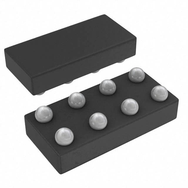
The SN74AUC2G240YZPR is available in a small-outline package (SOP) with 8 pins.
Essence
The essence of this product lies in its ability to amplify and buffer signals efficiently, ensuring reliable and accurate data transmission.
Packaging/Quantity
The SN74AUC2G240YZPR is typically packaged in reels or tubes, with a quantity of 2500 units per reel/tube.
Specifications
- Supply Voltage: 1.65V to 3.6V
- Input Voltage Range: 0V to VCC
- Output Voltage Range: 0V to VCC
- Operating Temperature Range: -40°C to +85°C
- Input Capacitance: 3.5pF
- Output Capacitance: 4.5pF
- Propagation Delay Time: 2.7ns (max)
- Output Current: ±24mA
Detailed Pin Configuration
The SN74AUC2G240YZPR has the following pin configuration:
```
| | --| A1 VCC|-- --| A2 B1 |-- --| GND OE |-- --| Y1 A3 |-- --| Y2 B2 |-- --| GND Y3 |-- --| B3 GND |-- |___________| ```
Functional Features
- Dual 2-input NOR gate functionality
- High-speed operation for efficient signal processing
- Low power consumption for energy-efficient designs
- Wide operating voltage range allows compatibility with various systems
- RoHS compliant, ensuring environmental friendliness
Advantages and Disadvantages
Advantages
- High-speed operation enables quick data transmission
- Low power consumption prolongs battery life in portable devices
- Small package size saves valuable board space
- Wide operating voltage range provides flexibility in system design
Disadvantages
- Limited number of inputs and outputs restricts the complexity of circuits that can be built using this IC
- Propagation delay time may introduce timing issues in certain applications
Working Principles
The SN74AUC2G240YZPR operates based on the principles of logic gates. It consists of two 2-input NOR gates that amplify and buffer input signals. When the enable (OE) pin is high, the output pins (Y1 and Y2) reflect the logical NOR operation of the corresponding input pins (A1 and A2). Conversely, when the OE pin is low, the outputs are disabled, resulting in a high impedance state.
Detailed Application Field Plans
The SN74AUC2G240YZPR finds applications in various electronic devices and systems, including but not limited to: - Mobile phones - Tablets - Digital cameras - Portable media players - Automotive electronics - Industrial control systems
Detailed and Complete Alternative Models
- SN74AUC2G241YZPR
- SN74AUC2G242YZPR
- SN74AUC2G243YZPR
- SN74AUC2G244YZPR
- SN74AUC2G245YZPR
These alternative models offer similar functionality and characteristics, providing designers with options based on specific requirements.
In conclusion, the SN74AUC2G240YZPR is a versatile integrated circuit that offers high-speed signal amplification and buffering capabilities. Its low power consumption, small package size, and wide operating voltage range make it suitable for various applications in the electronics industry. While it has certain limitations, such as a limited number of inputs and outputs, its advantages outweigh the disadvantages. Designers can also consider alternative models within the same product family to meet specific design requirements.
기술 솔루션에 SN74AUC2G240YZPR 적용과 관련된 10가지 일반적인 질문과 답변을 나열하세요.
Sure! Here are 10 common questions and answers related to the application of SN74AUC2G240YZPR in technical solutions:
Q: What is SN74AUC2G240YZPR? A: SN74AUC2G240YZPR is a dual buffer/line driver IC (integrated circuit) that can be used for signal buffering and level shifting in various electronic applications.
Q: What is the operating voltage range of SN74AUC2G240YZPR? A: The operating voltage range of SN74AUC2G240YZPR is typically between 0.8V and 3.6V, making it suitable for low-power and battery-operated devices.
Q: Can SN74AUC2G240YZPR handle bi-directional signals? A: Yes, SN74AUC2G240YZPR supports bidirectional signal flow, allowing it to be used for both input and output buffering.
Q: What is the maximum output current of SN74AUC2G240YZPR? A: The maximum output current of SN74AUC2G240YZPR is typically around 24mA, which makes it capable of driving standard CMOS or TTL logic levels.
Q: Does SN74AUC2G240YZPR have built-in ESD protection? A: Yes, SN74AUC2G240YZPR incorporates built-in ESD (electrostatic discharge) protection, which helps safeguard against damage from static electricity.
Q: Can SN74AUC2G240YZPR be used in high-speed applications? A: Yes, SN74AUC2G240YZPR is designed for high-speed operation and can support data rates up to several hundred megahertz (MHz).
Q: What is the package type of SN74AUC2G240YZPR? A: SN74AUC2G240YZPR comes in a small footprint package known as DSBGA (Dual Small Ball Grid Array), which is suitable for space-constrained designs.
Q: Is SN74AUC2G240YZPR RoHS compliant? A: Yes, SN74AUC2G240YZPR is RoHS (Restriction of Hazardous Substances) compliant, ensuring it meets environmental regulations.
Q: Can SN74AUC2G240YZPR be used in automotive applications? A: Yes, SN74AUC2G240YZPR is qualified for automotive applications and can operate reliably in automotive temperature ranges.
Q: Are there any application notes or reference designs available for SN74AUC2G240YZPR? A: Yes, Texas Instruments provides application notes and reference designs that showcase the usage of SN74AUC2G240YZPR in various technical solutions. These resources can help with circuit design and implementation.
Please note that the answers provided here are general and may vary depending on specific datasheet specifications and application requirements.