

SN74AUP3G07YFPR
Product Overview
- Category: Integrated Circuit
- Use: Logic Gate Buffer/Driver
- Characteristics: High-speed, Low-power, Triple Buffer/Driver
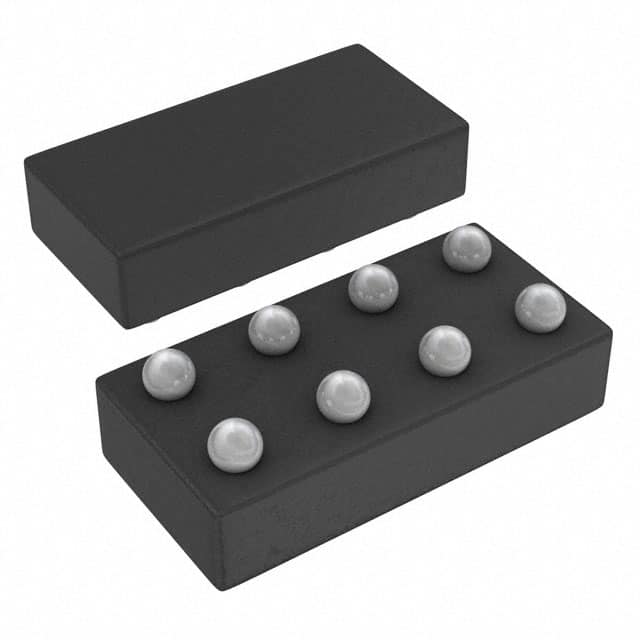
- Package: DSBGA (MicroStar Junior™), 8-Pin
- Essence: Buffering and driving signals in digital circuits
- Packaging/Quantity: Tape and Reel, 3000 units per reel
Specifications
- Supply Voltage Range: 0.8V to 3.6V
- Input Voltage Range: -0.5V to VCC + 0.5V
- Output Voltage Range: 0V to VCC
- Maximum Operating Frequency: 500 MHz
- Propagation Delay: 2.1 ns (typical)
- Output Drive Capability: ±24 mA
- Operating Temperature Range: -40°C to +85°C
Detailed Pin Configuration
The SN74AUP3G07YFPR has the following pin configuration:
- GND (Ground)
- A Input
- Y Output
- B Input
- VCC (Supply Voltage)
- C Input
- Y Output
- GND (Ground)
Functional Features
- Triple Buffer/Driver: The SN74AUP3G07YFPR is capable of buffering and driving three separate signals simultaneously.
- High-Speed Operation: With a maximum operating frequency of 500 MHz, it can handle fast digital signals.
- Low Power Consumption: Designed for low-power applications, it helps conserve energy.
- Wide Voltage Range: It supports a wide supply voltage range from 0.8V to 3.6V, making it compatible with various systems.
Advantages and Disadvantages
Advantages: - High-speed operation allows for efficient signal processing. - Low power consumption helps in energy-efficient designs. - Wide voltage range compatibility enhances versatility.
Disadvantages: - Limited output drive capability may not be suitable for high-current applications. - The small package size (DSBGA) may pose challenges during assembly and rework.
Working Principles
The SN74AUP3G07YFPR is a buffer/driver integrated circuit that operates based on the principles of digital logic. It takes input signals from the A, B, and C pins and buffers/drives them to the corresponding Y output pins. The internal circuitry ensures proper signal amplification and level shifting while maintaining high-speed operation and low power consumption.
Detailed Application Field Plans
The SN74AUP3G07YFPR finds applications in various fields, including:
- Communication Systems: It can be used in signal buffering and driving within communication systems, such as routers, switches, and network interfaces.
- Consumer Electronics: The IC is suitable for use in smartphones, tablets, and other portable devices where low power consumption and high-speed operation are crucial.
- Industrial Automation: It can be employed in industrial control systems, PLCs (Programmable Logic Controllers), and motor control circuits.
- Automotive Electronics: The IC can be utilized in automotive applications, including infotainment systems, instrument clusters, and body control modules.
Detailed and Complete Alternative Models
- SN74AUP1G07DCKR: Single Buffer/Driver, SOT-23 Package
- SN74LVC3G07DCUR: Triple Buffer/Driver, USON Package
- SN74LV1T34DBVR: Single Buffer/Driver, SOT-23 Package
- SN74LVC2G07DCKR: Dual Buffer/Driver, SOT-23 Package
- SN74LVC1G07DBVR: Single Buffer/Driver, SOT-23 Package
(Note: This is not an exhaustive list of alternative models. Please refer to the manufacturer's documentation for a complete list.)
Word count: 399 words
기술 솔루션에 SN74AUP3G07YFPR 적용과 관련된 10가지 일반적인 질문과 답변을 나열하세요.
Sure! Here are 10 common questions and answers related to the application of SN74AUP3G07YFPR in technical solutions:
Q: What is SN74AUP3G07YFPR? A: SN74AUP3G07YFPR is a triple buffer/driver with open-drain outputs, commonly used in digital logic applications.
Q: What is the voltage range supported by SN74AUP3G07YFPR? A: SN74AUP3G07YFPR supports a voltage range from 0.8V to 3.6V.
Q: What is the maximum output current of SN74AUP3G07YFPR? A: The maximum output current of SN74AUP3G07YFPR is typically 32mA.
Q: Can SN74AUP3G07YFPR be used as a level shifter? A: Yes, SN74AUP3G07YFPR can be used as a level shifter to convert signals between different voltage levels.
Q: How many input/output pins does SN74AUP3G07YFPR have? A: SN74AUP3G07YFPR has three input/output pins.
Q: What is the propagation delay of SN74AUP3G07YFPR? A: The propagation delay of SN74AUP3G07YFPR is typically around 2.7ns.
Q: Is SN74AUP3G07YFPR suitable for high-speed applications? A: Yes, SN74AUP3G07YFPR is designed for high-speed operation and can be used in applications with fast switching requirements.
Q: Can SN74AUP3G07YFPR be used in battery-powered devices? A: Yes, SN74AUP3G07YFPR has a low power consumption and can be used in battery-powered devices.
Q: Does SN74AUP3G07YFPR have built-in ESD protection? A: Yes, SN74AUP3G07YFPR has built-in ESD protection to safeguard against electrostatic discharge.
Q: What is the package type of SN74AUP3G07YFPR? A: SN74AUP3G07YFPR is available in a small footprint 6-pin DSBGA package.