

SN74LVC1G17YZVR
Product Overview
- Category: Integrated Circuit (IC)
- Use: Logic Gate
- Characteristics: Single Schmitt-Trigger Buffer/Driver
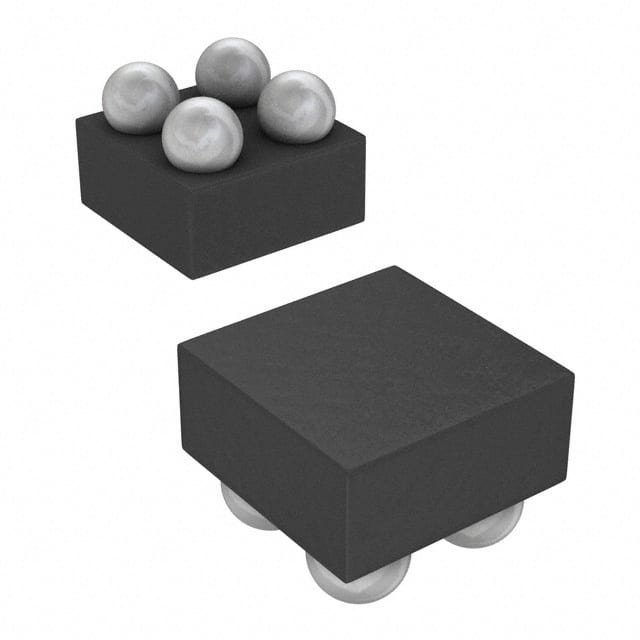
- Package: SOT-23-5
- Essence: The SN74LVC1G17YZVR is a single Schmitt-trigger buffer/driver designed for 1.65V to 5.5V VCC operation.
- Packaging/Quantity: Tape and Reel, 3000 pieces per reel
Specifications
- Supply Voltage Range: 1.65V to 5.5V
- Input Voltage Range: 0V to VCC
- Output Voltage Range: 0V to VCC
- Operating Temperature Range: -40°C to +125°C
- Propagation Delay: 4.3ns (typical) at 3.3V
- Output Drive Capability: ±24mA at 3.3V
- Input Hysteresis: 0.25V (typical) at 3.3V
Detailed Pin Configuration
The SN74LVC1G17YZVR has the following pin configuration:
```
/ \ | 1 | ______/ ```
Pin 1: Input (A) Pin 2: Ground (GND) Pin 3: Output (Y) Pin 4: Power Supply (VCC) Pin 5: Not Connected (NC)
Functional Features
- Single Schmitt-trigger buffer/driver with open-drain output
- Provides hysteresis for improved noise immunity
- Supports bidirectional data flow
- Low power consumption
- High-speed operation
- Compatible with various logic families
Advantages and Disadvantages
Advantages: - Improved noise immunity due to hysteresis - Wide supply voltage range allows for versatile applications - Small package size enables space-saving designs - Low power consumption
Disadvantages: - Limited output drive capability compared to some other ICs - Single-channel design may not be suitable for applications requiring multiple inputs/outputs
Working Principles
The SN74LVC1G17YZVR is a single Schmitt-trigger buffer/driver. It takes an input signal and provides an output signal with improved noise immunity. The Schmitt-trigger input ensures that the output transitions occur at different voltage levels for rising and falling input signals, providing hysteresis.
Detailed Application Field Plans
The SN74LVC1G17YZVR can be used in various applications, including but not limited to:
- Signal Conditioning: The Schmitt-trigger input helps clean up noisy signals, making it suitable for applications where signal conditioning is required.
- Level Shifting: The wide supply voltage range allows for level shifting between different logic families or voltage domains.
- Sensor Interfaces: The buffer/driver can be used to interface sensors with microcontrollers or other digital devices, ensuring reliable signal transmission.
- Communication Systems: The open-drain output makes it compatible with bus systems, such as I2C or SMBus.
Detailed and Complete Alternative Models
Some alternative models to the SN74LVC1G17YZVR include:
- SN74LVC1G17DBVR: Similar specifications and functionality, but in a different package (SOT-23-6).
- SN74LVC1G17DCKR: Similar specifications and functionality, but in a different package (SC-70-5).
- SN74LVC1G17DRLR: Similar specifications and functionality, but in a different package (SOT-553).
These alternative models provide flexibility in terms of package options while maintaining similar performance characteristics.
Word count: 399 words
기술 솔루션에 SN74LVC1G17YZVR 적용과 관련된 10가지 일반적인 질문과 답변을 나열하세요.
Sure! Here are 10 common questions and answers related to the application of SN74LVC1G17YZVR:
Q1: What is SN74LVC1G17YZVR? A1: SN74LVC1G17YZVR is a single Schmitt-trigger buffer/driver with open-drain output, commonly used in digital logic circuits.
Q2: What is the voltage supply range for SN74LVC1G17YZVR? A2: The voltage supply range for SN74LVC1G17YZVR is typically between 1.65V and 5.5V.
Q3: What is the maximum output current of SN74LVC1G17YZVR? A3: The maximum output current of SN74LVC1G17YZVR is typically 32mA.
Q4: Can SN74LVC1G17YZVR be used as a level shifter? A4: Yes, SN74LVC1G17YZVR can be used as a level shifter to convert signals between different voltage levels.
Q5: What is the input voltage threshold for SN74LVC1G17YZVR? A5: The input voltage threshold for SN74LVC1G17YZVR is typically 0.8V.
Q6: Is SN74LVC1G17YZVR suitable for high-speed applications? A6: Yes, SN74LVC1G17YZVR is designed for high-speed operation and can be used in applications with fast switching requirements.
Q7: Can SN74LVC1G17YZVR drive capacitive loads? A7: Yes, SN74LVC1G17YZVR can drive small capacitive loads, but it is recommended to add series resistors to limit the current during charging and discharging.
Q8: What is the maximum propagation delay of SN74LVC1G17YZVR? A8: The maximum propagation delay of SN74LVC1G17YZVR is typically 4.5ns.
Q9: Can SN74LVC1G17YZVR be used in battery-powered applications? A9: Yes, SN74LVC1G17YZVR has a low power consumption and can be used in battery-powered applications.
Q10: Is SN74LVC1G17YZVR available in different package options? A10: Yes, SN74LVC1G17YZVR is available in various package options, such as SOT-23 and DSBGA, to suit different application requirements.
Please note that the answers provided here are general and may vary depending on specific datasheet specifications and application conditions.