

SN74LVC1G80YEPR
Product Overview
- Category: Integrated Circuit
- Use: Logic Gate
- Characteristics: Single Positive-Edge-Triggered D-Type Flip-Flop
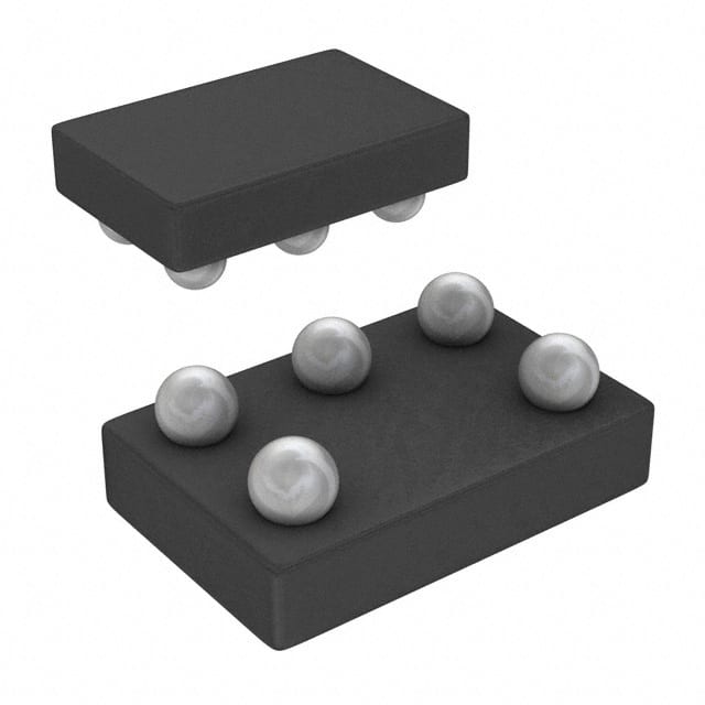
- Package: 6-Bump DSBGA (0.8mm x 0.8mm)
- Essence: Flip-flop circuit for storing a single bit of data
- Packaging/Quantity: Tape and Reel, 3000 units per reel
Specifications
- Supply Voltage Range: 1.65V to 5.5V
- High-Level Input Voltage: 0.7 x VCC
- Low-Level Input Voltage: 0.3 x VCC
- High-Level Output Voltage: 0.9 x VCC
- Low-Level Output Voltage: 0.1 x VCC
- Maximum Operating Frequency: 100 MHz
- Propagation Delay: 4.2 ns (typical)
Detailed Pin Configuration
The SN74LVC1G80YEPR has the following pin configuration:
____
CLR   |    |
CLK   |    |
D     |    |
Q     |    |
GND   |    |
VCC   |____|
Functional Features
- Single positive-edge-triggered D-type flip-flop
- Asynchronous clear input (CLR) for resetting the flip-flop
- Synchronous clock input (CLK) for triggering the flip-flop
- Data input (D) for setting the flip-flop state
- Output (Q) provides the stored value of the flip-flop
- Wide supply voltage range allows compatibility with various systems
Advantages and Disadvantages
Advantages: - Small package size enables space-saving designs - Wide supply voltage range enhances versatility - High operating frequency allows for fast data processing - Asynchronous clear input provides flexibility in resetting the flip-flop
Disadvantages: - Limited to storing a single bit of data - Not suitable for applications requiring multiple flip-flops or complex logic operations
Working Principles
The SN74LVC1G80YEPR is a positive-edge-triggered D-type flip-flop. It stores a single bit of data and can be set or reset based on the inputs provided. The CLK input triggers the flip-flop, causing it to capture the value present at the D input. The CLR input asynchronously resets the flip-flop, forcing the Q output to a low state. The stored value remains unchanged until the next clock edge triggers a new data capture.
Detailed Application Field Plans
The SN74LVC1G80YEPR is commonly used in various digital systems where the storage of a single bit of data is required. Some specific application fields include:
- Communication Systems: Used in data transmission circuits for buffering and synchronization purposes.
- Control Systems: Employed in control units to store control signals or status information.
- Consumer Electronics: Integrated into portable devices for power management and signal processing.
- Automotive Electronics: Utilized in vehicle control modules for storing sensor data or control parameters.
- Industrial Automation: Incorporated in programmable logic controllers (PLCs) for sequential logic operations.
Detailed and Complete Alternative Models
- SN74LVC1G80DCKR: SOT-23 package, similar specifications and features.
- MC74VHC1G80DF1G: SC-70 package, compatible functionality with additional ESD protection.
- TC7SET80FU: SOT-353 package, comparable performance with lower power consumption.
These alternative models offer similar functionality and can be considered as replacements for the SN74LVC1G80YEPR in different applications.
Word count: 420 words
기술 솔루션에 SN74LVC1G80YEPR 적용과 관련된 10가지 일반적인 질문과 답변을 나열하세요.
Sure! Here are 10 common questions and answers related to the application of SN74LVC1G80YEPR:
Q1: What is SN74LVC1G80YEPR? A1: SN74LVC1G80YEPR is a single positive-edge-triggered D-type flip-flop with reset. It is a logic IC used in digital circuits.
Q2: What is the operating voltage range for SN74LVC1G80YEPR? A2: The operating voltage range for SN74LVC1G80YEPR is typically between 1.65V and 5.5V.
Q3: What is the maximum clock frequency supported by SN74LVC1G80YEPR? A3: SN74LVC1G80YEPR can support clock frequencies up to 100 MHz.
Q4: Can SN74LVC1G80YEPR be used as a standalone component? A4: Yes, SN74LVC1G80YEPR can be used as a standalone component or integrated into larger circuit designs.
Q5: What is the typical power consumption of SN74LVC1G80YEPR? A5: The typical power consumption of SN74LVC1G80YEPR is low, making it suitable for battery-powered applications.
Q6: How many inputs and outputs does SN74LVC1G80YEPR have? A6: SN74LVC1G80YEPR has one data input (D), one clock input (CLK), one reset input (RST), and one output (Q).
Q7: Can SN74LVC1G80YEPR be cascaded to create larger flip-flop configurations? A7: Yes, multiple SN74LVC1G80YEPR flip-flops can be cascaded to create larger configurations.
Q8: What is the propagation delay of SN74LVC1G80YEPR? A8: The propagation delay of SN74LVC1G80YEPR is typically around 3.5 ns.
Q9: Can SN74LVC1G80YEPR be used in high-speed applications? A9: Yes, SN74LVC1G80YEPR is designed for high-speed operation and can be used in various high-frequency applications.
Q10: Are there any special considerations when using SN74LVC1G80YEPR in a circuit? A10: It is important to ensure proper decoupling and power supply filtering to minimize noise and ensure reliable operation.
Please note that these answers are general and may vary depending on specific application requirements.