

SN74LVC2G240YZPR
Product Overview
- Category: Integrated Circuit
- Use: Logic Gate
- Characteristics: Dual Buffer/Driver, Non-Inverting, 3-State Output
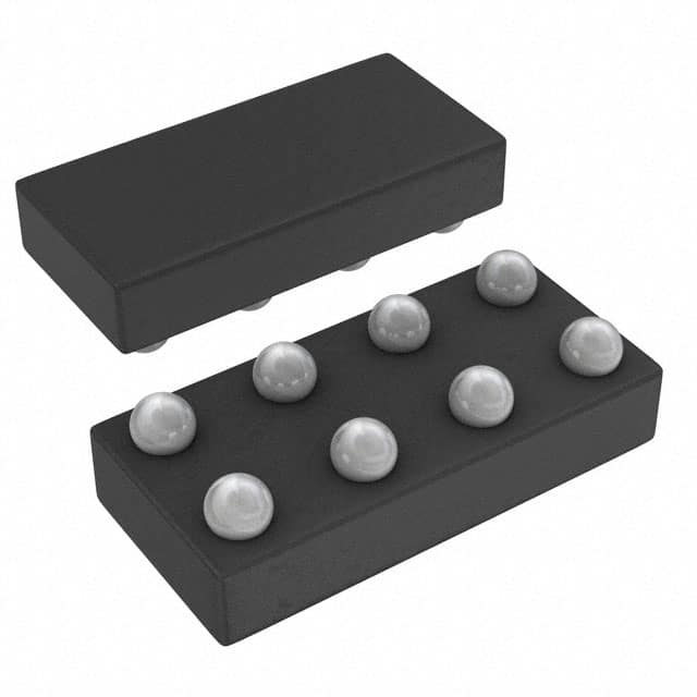
- Package: 8-Bump DSBGA (0.8mm x 1.2mm)
- Essence: The SN74LVC2G240YZPR is a dual buffer/driver designed for 2.3V to 5.5V VCC operation.
- Packaging/Quantity: Tape and Reel, 3000 pieces per reel
Specifications
- Supply Voltage Range: 2.3V to 5.5V
- Input Voltage Range: 0V to VCC
- Output Voltage Range: 0V to VCC
- Operating Temperature Range: -40°C to +85°C
- Propagation Delay: 4.7ns (typical)
- Output Drive Capability: ±24mA at 3.3V
- Input Capacitance: 3pF (typical)
Detailed Pin Configuration
The SN74LVC2G240YZPR has a total of 8 pins:
- A Input
- Y Output
- B Input
- GND (Ground)
- Y Output
- B Input
- A Input
- VCC (Power Supply)
Functional Features
- Dual non-inverting buffer/driver with 3-state output
- High-speed operation suitable for various applications
- Supports mixed-mode signal operation on all ports
- Low static power consumption
- Latch-up performance exceeds 100mA per JESD 78, Class II
Advantages and Disadvantages
Advantages
- Wide supply voltage range allows compatibility with different systems
- High-speed operation enables efficient data transmission
- 3-state output provides flexibility in controlling bus lines
- Low static power consumption reduces energy consumption
Disadvantages
- Limited number of inputs and outputs (dual buffer/driver)
- Small package size may require careful handling during assembly
Working Principles
The SN74LVC2G240YZPR is a dual buffer/driver integrated circuit that amplifies and buffers digital signals. It operates within a supply voltage range of 2.3V to 5.5V, making it compatible with various systems. The device features non-inverting inputs and outputs, allowing for signal amplification without changing the logic level.
The 3-state output feature enables the device to be connected to a common bus line, where multiple devices can share the same communication channel. This allows for efficient data transmission and control.
The SN74LVC2G240YZPR has low static power consumption, making it suitable for battery-powered applications. Its latch-up performance exceeds industry standards, ensuring reliable operation even in challenging conditions.
Detailed Application Field Plans
The SN74LVC2G240YZPR is widely used in various applications, including:
Communication Systems: The device is utilized in data communication systems to amplify and buffer digital signals, ensuring reliable transmission between different components.
Industrial Automation: In industrial automation systems, the SN74LVC2G240YZPR is employed to interface between different modules, enabling efficient control and communication.
Consumer Electronics: The device finds application in consumer electronics such as smartphones, tablets, and gaming consoles, where it helps in signal amplification and buffering.
Automotive Electronics: Due to its wide supply voltage range and high-speed operation, the SN74LVC2G240YZPR is suitable for automotive electronics, including infotainment systems, instrument clusters, and body control modules.
Detailed and Complete Alternative Models
- SN74LVC2G07: Dual Buffer/Driver with Open-Drain Outputs
- SN74LVC2G17: Dual Schmitt-Trigger Buffer/Driver
- SN74LVC2G34: Dual Buffer/Driver with 3-State Outputs
- SN74LVC2G125: Dual Bus Buffer Gate with 3-State Outputs
These alternative models offer similar functionality to the SN74LVC2G240YZPR, providing options for different design requirements.
In conclusion, the SN74LVC2G240YZPR is a dual buffer/driver integrated circuit that offers high-speed operation, low power consumption, and compatibility with various systems. Its versatile applications make it a popular choice in communication systems, industrial automation, consumer electronics, and automotive electronics.
기술 솔루션에 SN74LVC2G240YZPR 적용과 관련된 10가지 일반적인 질문과 답변을 나열하세요.
Sure! Here are 10 common questions and answers related to the application of SN74LVC2G240YZPR:
Q: What is SN74LVC2G240YZPR? A: SN74LVC2G240YZPR is a dual buffer and line driver IC (integrated circuit) that can be used in various technical solutions.
Q: What is the voltage range supported by SN74LVC2G240YZPR? A: SN74LVC2G240YZPR supports a voltage range from 1.65V to 5.5V.
Q: What is the maximum output current of SN74LVC2G240YZPR? A: The maximum output current of SN74LVC2G240YZPR is typically 24mA.
Q: Can SN74LVC2G240YZPR be used for level shifting applications? A: Yes, SN74LVC2G240YZPR can be used for level shifting between different voltage domains.
Q: Does SN74LVC2G240YZPR have built-in ESD protection? A: Yes, SN74LVC2G240YZPR has built-in ESD (electrostatic discharge) protection to safeguard against static electricity.
Q: What is the operating temperature range of SN74LVC2G240YZPR? A: SN74LVC2G240YZPR can operate within a temperature range of -40°C to +85°C.
Q: How many input/output pins does SN74LVC2G240YZPR have? A: SN74LVC2G240YZPR has two input pins and two output pins.
Q: Can SN74LVC2G240YZPR be used in battery-powered applications? A: Yes, SN74LVC2G240YZPR can be used in battery-powered applications due to its low power consumption.
Q: Is SN74LVC2G240YZPR compatible with other logic families? A: Yes, SN74LVC2G240YZPR is compatible with a wide range of logic families, including TTL and CMOS.
Q: What is the package type of SN74LVC2G240YZPR? A: SN74LVC2G240YZPR comes in a small-outline transistor (SOT) package, specifically SOT-23-8.
Please note that these answers are general and may vary depending on specific datasheet specifications and application requirements.