

SN74LVC2G241YZPR
Product Overview
- Category: Integrated Circuit
- Use: Logic Gate Buffer/Driver
- Characteristics: Low Voltage, Dual Gate, Non-Inverting
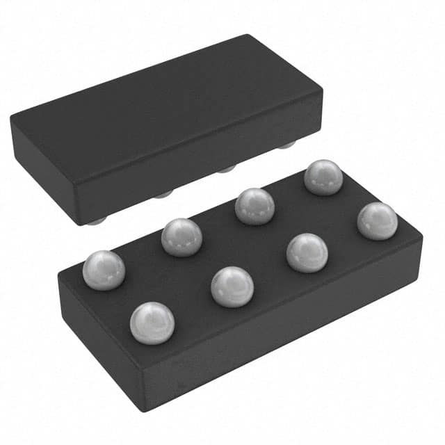
- Package: 8-pin DSBGA (MicroStar Junior™), Tape and Reel
- Essence: This integrated circuit is a dual gate buffer/driver designed for low voltage applications.
- Packaging/Quantity: Available in tape and reel packaging with a quantity of 3000 units per reel.
Specifications
- Supply Voltage Range: 1.65V to 5.5V
- Input Voltage Range: 0V to VCC
- Output Voltage Range: 0V to VCC
- Operating Temperature Range: -40°C to +85°C
- Propagation Delay: 3.9ns (typical)
- Output Drive Capability: ±24mA
- Input Capacitance: 3pF (typical)
Pin Configuration
The SN74LVC2G241YZPR has the following pin configuration:
___________
   A1 |           | VCC
   A2 |           | B1
   GND |           | B2
   OE  |           | A1
   B1  |           | A2
   B2  |           | GND
   VCC |           | OE
       ¯¯¯¯¯¯¯¯¯¯¯
Functional Features
- Dual gate buffer/driver with non-inverting outputs
- Supports wide supply voltage range from 1.65V to 5.5V
- High-speed operation with low propagation delay
- Provides high output drive capability
- Low input capacitance for reduced power consumption
Advantages and Disadvantages
Advantages
- Wide supply voltage range allows compatibility with various systems
- High-speed operation enables efficient signal processing
- Non-inverting outputs simplify circuit design
- Low input capacitance reduces power consumption
Disadvantages
- Limited output drive capability compared to some other models
- Not suitable for high-voltage applications
Working Principles
The SN74LVC2G241YZPR operates as a buffer/driver by amplifying and shaping digital signals. It accepts logic level inputs and provides non-inverted outputs. The device is designed to operate within a wide range of supply voltages, making it suitable for use in diverse electronic systems.
Detailed Application Field Plans
The SN74LVC2G241YZPR can be used in various applications, including:
- Battery-powered devices: The low voltage operation and low power consumption make it ideal for portable electronics.
- Communication systems: The high-speed operation and non-inverting outputs are beneficial for signal transmission and reception.
- Industrial automation: The wide supply voltage range and high output drive capability enable interfacing with different control systems.
- Automotive electronics: The device's temperature range and compact package make it suitable for automotive applications.
Detailed and Complete Alternative Models
- SN74LVC2G07: Dual Buffer/Driver with Open-Drain Outputs
- SN74LVC2G17: Dual Schmitt-Trigger Buffer/Driver
- SN74LVC2G34: Dual Buffer/Driver with 3-State Outputs
- SN74LVC2G125: Dual Bus Buffer/Driver with 3-State Outputs
These alternative models offer similar functionality and can be considered as alternatives to the SN74LVC2G241YZPR based on specific application requirements.
In conclusion, the SN74LVC2G241YZPR is a dual gate buffer/driver integrated circuit designed for low voltage applications. It offers high-speed operation, wide supply voltage range, and non-inverting outputs. While it has limitations in output drive capability and high-voltage applications, it finds extensive use in battery-powered devices, communication systems, industrial automation, and automotive electronics. Alternative models with similar functionality are also available in the market.
Word count: 459
기술 솔루션에 SN74LVC2G241YZPR 적용과 관련된 10가지 일반적인 질문과 답변을 나열하세요.
Sure! Here are 10 common questions and answers related to the application of SN74LVC2G241YZPR:
Q: What is SN74LVC2G241YZPR? A: SN74LVC2G241YZPR is a dual buffer/driver IC (integrated circuit) that can be used for signal buffering and level shifting in various technical solutions.
Q: What is the voltage range supported by SN74LVC2G241YZPR? A: SN74LVC2G241YZPR supports a voltage range from 1.65V to 5.5V, making it compatible with a wide range of devices and systems.
Q: Can SN74LVC2G241YZPR be used for bidirectional communication? A: Yes, SN74LVC2G241YZPR supports bidirectional communication, allowing signals to be transmitted in both directions.
Q: What is the maximum output current of SN74LVC2G241YZPR? A: SN74LVC2G241YZPR has a maximum output current of 24mA, which makes it suitable for driving various loads.
Q: Is SN74LVC2G241YZPR compatible with I2C and SPI protocols? A: Yes, SN74LVC2G241YZPR is compatible with both I2C and SPI protocols, making it useful for interfacing with devices that use these protocols.
Q: Can SN74LVC2G241YZPR be used in battery-powered applications? A: Yes, SN74LVC2G241YZPR is designed to operate efficiently in low-power applications, including battery-powered devices.
Q: Does SN74LVC2G241YZPR have built-in ESD protection? A: Yes, SN74LVC2G241YZPR has built-in ESD (Electrostatic Discharge) protection, which helps to safeguard the IC from damage caused by static electricity.
Q: What is the package type of SN74LVC2G241YZPR? A: SN74LVC2G241YZPR comes in a small and compact 8-pin DSBGA (MicroStar Junior™) package, which is suitable for space-constrained applications.
Q: Can SN74LVC2G241YZPR be used in automotive applications? A: Yes, SN74LVC2G241YZPR is qualified for automotive applications and meets the necessary standards for automotive electronics.
Q: Where can I find more information about the application of SN74LVC2G241YZPR? A: You can refer to the datasheet provided by the manufacturer or visit their official website for detailed information on the application of SN74LVC2G241YZPR.
Please note that these answers are general and may vary depending on specific use cases and requirements. It's always recommended to consult the datasheet and relevant technical documentation for accurate information.