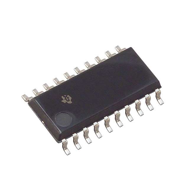
SN74LVC573ANSRE4
Product Overview
Category
SN74LVC573ANSRE4 belongs to the category of integrated circuits (ICs).
Use
It is commonly used as an octal transparent latch with 3-state outputs.
Characteristics
- Octal D-type transparent latches
- 3-state outputs for bus-oriented applications
- High-speed operation
- Low power consumption
- Schmitt-trigger inputs for noise immunity
- Available in surface mount package
Package
SN74LVC573ANSRE4 is available in a small-outline integrated circuit (SOIC) package.
Essence
The essence of SN74LVC573ANSRE4 lies in its ability to store and output data in a digital system, making it suitable for various applications.
Packaging/Quantity
SN74LVC573ANSRE4 is typically packaged in reels or tubes, with a quantity of 2500 units per reel/tube.
Specifications
- Supply voltage: 1.65V to 5.5V
- Input voltage range: -0.5V to VCC + 0.5V
- Output voltage range: -0.5V to VCC + 0.5V
- Operating temperature range: -40°C to +85°C
- Output current: ±32mA
- Propagation delay: 3.8ns (typical)
Detailed Pin Configuration
The pin configuration of SN74LVC573ANSRE4 is as follows:
- GND (Ground)
- D0 (Data input 0)
- D1 (Data input 1)
- D2 (Data input 2)
- D3 (Data input 3)
- D4 (Data input 4)
- D5 (Data input 5)
- D6 (Data input 6)
- D7 (Data input 7)
- OE (Output enable)
- LE (Latch enable)
- Q0 (Output 0)
- Q1 (Output 1)
- Q2 (Output 2)
- Q3 (Output 3)
- Q4 (Output 4)
- Q5 (Output 5)
- Q6 (Output 6)
- Q7 (Output 7)
- VCC (Supply voltage)
Functional Features
SN74LVC573ANSRE4 offers the following functional features:
- Octal transparent latch: Allows data to be stored and outputted on the rising edge of the latch enable signal.
- 3-state outputs: Enables bus-oriented applications by providing high impedance state when the output enable signal is low.
- Schmitt-trigger inputs: Provides noise immunity by ensuring a clean transition between logic levels.
Advantages and Disadvantages
Advantages
- High-speed operation: Suitable for applications requiring fast data transfer.
- Low power consumption: Helps in reducing overall power consumption of the system.
- Noise immunity: Schmitt-trigger inputs ensure reliable operation in noisy environments.
Disadvantages
- Limited output current: The maximum output current is ±32mA, which may not be sufficient for certain applications.
- Temperature limitations: The operating temperature range of -40°C to +85°C may restrict usage in extreme temperature conditions.
Working Principles
SN74LVC573ANSRE4 operates based on the principles of digital storage and output control. When the latch enable (LE) signal is high, the data inputs (D0-D7) are latched and stored. On the rising edge of the LE signal, the stored data is transferred to the corresponding outputs (Q0-Q7). The output enable (OE) signal controls the state of the outputs, allowing them to be either active or in a high impedance state.
Detailed Application Field Plans
SN74LVC573ANSRE4 finds applications in various fields, including:
- Microcontrollers: Used for interfacing with external devices and expanding input/output capabilities.
- Data communication systems: Enables data buffering and synchronization in communication protocols.
- Industrial automation: Facilitates control and monitoring of multiple devices in industrial settings.
- Automotive electronics: Supports data transfer and control functions in automotive systems.
- Consumer electronics: Used in digital appliances, gaming consoles, and other consumer electronic devices.
Detailed and Complete Alternative Models
Some alternative models that offer similar functionality to SN74LVC573ANSRE4 are:
- 74HC573: A popular CMOS octal latch with 3-state outputs.
- CD74HCT573: High-speed CMOS octal latch with 3-state outputs.
- MC74LVX573: Low-voltage CMOS octal latch with 3-state outputs.
These alternative models can be considered based on specific requirements and compatibility with the system design.
*Word count:
기술 솔루션에 SN74LVC573ANSRE4 적용과 관련된 10가지 일반적인 질문과 답변을 나열하세요.
Sure! Here are 10 common questions and answers related to the application of SN74LVC573ANSRE4:
Q: What is SN74LVC573ANSRE4? A: SN74LVC573ANSRE4 is a octal transparent D-type latch with 3-state outputs, commonly used in digital systems.
Q: What is the operating voltage range for SN74LVC573ANSRE4? A: The operating voltage range for SN74LVC573ANSRE4 is typically between 1.65V and 5.5V.
Q: What is the maximum output current that SN74LVC573ANSRE4 can handle? A: SN74LVC573ANSRE4 can handle a maximum output current of 32mA per channel.
Q: Can SN74LVC573ANSRE4 be used for bidirectional data transfer? A: No, SN74LVC573ANSRE4 is not designed for bidirectional data transfer. It is a unidirectional latch.
Q: How many input and output pins does SN74LVC573ANSRE4 have? A: SN74LVC573ANSRE4 has 8 input pins (D0-D7) and 8 output pins (Q0-Q7).
Q: What is the purpose of the 3-state outputs in SN74LVC573ANSRE4? A: The 3-state outputs allow multiple devices to share a common bus without interfering with each other.
Q: Can SN74LVC573ANSRE4 be cascaded to increase the number of latches? A: Yes, multiple SN74LVC573ANSRE4 latches can be cascaded together to increase the number of latches in a system.
Q: What is the maximum clock frequency that SN74LVC573ANSRE4 can support? A: SN74LVC573ANSRE4 can support clock frequencies up to 100MHz.
Q: Is SN74LVC573ANSRE4 suitable for high-speed applications? A: Yes, SN74LVC573ANSRE4 is designed for high-speed operation and is suitable for various applications including data storage and signal buffering.
Q: Are there any special considerations when using SN74LVC573ANSRE4 in noisy environments? A: It is recommended to use proper decoupling capacitors near the power supply pins of SN74LVC573ANSRE4 to minimize noise interference.
Please note that these answers are general and may vary depending on specific application requirements.


