

SN74LVC74ARGYRG4
Product Overview
- Category: Integrated Circuit (IC)
- Use: Flip-Flop
- Characteristics: Low-voltage, high-speed, dual D-type positive-edge-triggered flip-flop
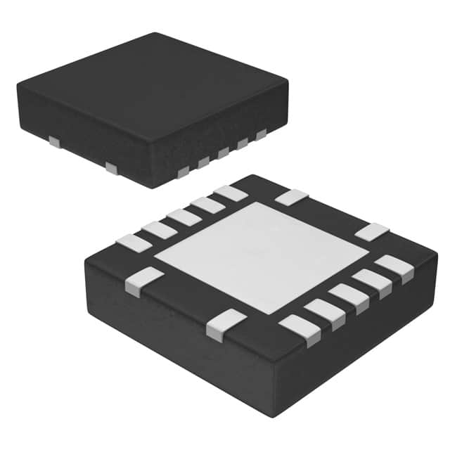
- Package: VQFN-20
- Essence: This IC is designed to store and transfer data in digital systems.
- Packaging/Quantity: Tape and Reel, 2500 units per reel
Specifications
- Supply Voltage Range: 1.65V to 5.5V
- High-Level Input Voltage: 2V to VCC + 0.5V
- Low-Level Input Voltage: -0.5V to 0.8V
- High-Level Output Voltage: VCC - 0.5V
- Low-Level Output Voltage: 0.5V
- Maximum Operating Frequency: 200MHz
- Propagation Delay Time: 3.7ns (typical)
- Operating Temperature Range: -40°C to 85°C
Detailed Pin Configuration
The SN74LVC74ARGYRG4 has a total of 20 pins arranged as follows:
__    __
   CLR |1  \/  20| VCC
   D   |2       19| Q
   CLK |3       18| Q'
   PR  |4       17| GND
   PRE |5       16| D'
   Q'  |6       15| CLK'
   Q   |7       14| CLR'
  GND  |8       13| PRE'
   D'  |9       12| PR'
  CLK' |10      11| OE#
        --    --
Functional Features
- Dual D-type positive-edge-triggered flip-flop with clear and preset inputs
- Supports asynchronous clear and preset operations
- High-speed operation with low power consumption
- Compatible with various logic families
- Provides data storage and transfer capabilities in digital systems
Advantages and Disadvantages
Advantages: - Low-voltage operation allows for compatibility with modern digital systems - High-speed performance enables efficient data processing - Dual flip-flop design provides flexibility in circuit design - Clear and preset inputs allow for easy initialization of the flip-flop
Disadvantages: - Limited operating temperature range (-40°C to 85°C) - Requires external clock signal for proper operation - Packaging may not be suitable for all applications
Working Principles
The SN74LVC74ARGYRG4 operates as a dual D-type positive-edge-triggered flip-flop. It stores and transfers data based on the rising edge of the clock signal. The clear (CLR) and preset (PR) inputs allow for asynchronous clearing and presetting of the flip-flop, respectively. The outputs (Q and Q') reflect the stored data and its complement.
Detailed Application Field Plans
The SN74LVC74ARGYRG4 is commonly used in various digital systems, including but not limited to:
- Microcontrollers: Used for storing and transferring data between different components of the microcontroller.
- Communication Systems: Enables data synchronization and buffering in communication protocols.
- Data Storage: Utilized in memory modules for data storage and retrieval operations.
- Industrial Automation: Facilitates control and sequencing of processes in industrial automation systems.
- Consumer Electronics: Integrated into electronic devices for data processing and control functions.
Detailed and Complete Alternative Models
- SN74LVC74APW: TSSOP-14 package, similar specifications and features.
- MC74VHC74DTR2G: SOIC-14 package, compatible functionality with additional features.
- CD74HC74M: PDIP-14 package, higher operating temperature range.
These alternative models offer similar functionality and can be used as replacements for the SN74LVC74ARGYRG4 in various applications.
Word count: 487 words
기술 솔루션에 SN74LVC74ARGYRG4 적용과 관련된 10가지 일반적인 질문과 답변을 나열하세요.
Sure! Here are 10 common questions and answers related to the application of SN74LVC74ARGYRG4:
Q: What is SN74LVC74ARGYRG4? A: SN74LVC74ARGYRG4 is a dual positive-edge-triggered D-type flip-flop integrated circuit (IC) that can store one bit of data.
Q: What is the voltage range supported by SN74LVC74ARGYRG4? A: SN74LVC74ARGYRG4 supports a wide voltage range from 1.65V to 5.5V, making it compatible with various logic families.
Q: How many flip-flops are there in SN74LVC74ARGYRG4? A: SN74LVC74ARGYRG4 contains two independent flip-flops, allowing it to store two bits of data.
Q: What is the maximum clock frequency supported by SN74LVC74ARGYRG4? A: SN74LVC74ARGYRG4 can operate at a maximum clock frequency of 100 MHz, enabling high-speed data storage and retrieval.
Q: Can SN74LVC74ARGYRG4 be used for synchronous or asynchronous applications? A: SN74LVC74ARGYRG4 is primarily designed for synchronous applications, where data is stored and retrieved based on clock signals.
Q: What is the power supply voltage required for SN74LVC74ARGYRG4? A: SN74LVC74ARGYRG4 requires a power supply voltage between 1.65V and 5.5V, depending on the desired logic levels.
Q: Does SN74LVC74ARGYRG4 support tri-state outputs? A: Yes, SN74LVC74ARGYRG4 supports tri-state outputs, allowing multiple devices to share a common bus without interference.
Q: Can SN74LVC74ARGYRG4 be used in battery-powered applications? A: Yes, SN74LVC74ARGYRG4's low power consumption and wide voltage range make it suitable for battery-powered applications.
Q: What is the package type of SN74LVC74ARGYRG4? A: SN74LVC74ARGYRG4 comes in a small-outline integrated circuit (SOIC) package with 14 pins.
Q: Are there any specific application notes or reference designs available for SN74LVC74ARGYRG4? A: Yes, Texas Instruments provides application notes and reference designs that can help in implementing SN74LVC74ARGYRG4 in various technical solutions.
Please note that these answers are general and may vary depending on the specific requirements and use cases. It is always recommended to refer to the datasheet and documentation provided by the manufacturer for accurate information.