

TPS61201DRCT
Product Overview
Category
The TPS61201DRCT belongs to the category of integrated circuits (ICs) and specifically falls under the voltage regulators - switching regulators classification.
Use
This product is primarily used for boosting or stepping up voltage levels efficiently. It is commonly employed in various electronic devices and systems where a higher voltage level is required.
Characteristics
- High efficiency: The TPS61201DRCT offers high conversion efficiency, ensuring minimal power loss during voltage conversion.
- Wide input voltage range: It can accept input voltages ranging from 0.3V to 5.5V, making it suitable for a wide range of applications.
- Adjustable output voltage: The output voltage can be adjusted within a specific range to meet the requirements of different applications.
- Low quiescent current: The device has a low quiescent current, which helps conserve power when the load is light or inactive.
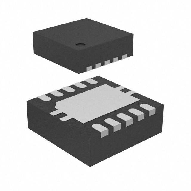
Package
The TPS61201DRCT is available in a small and compact package known as SON-6, which stands for Small Outline No-Lead 6-pin package. This package type offers ease of handling and efficient heat dissipation.
Essence
The essence of the TPS61201DRCT lies in its ability to efficiently step up voltage levels while maintaining high conversion efficiency and low power consumption.
Packaging/Quantity
The TPS61201DRCT is typically packaged in reels containing 2500 units per reel. This packaging format ensures easy handling and protection during transportation and storage.
Specifications
- Input Voltage Range: 0.3V to 5.5V
- Output Voltage Range: 1.8V to 5.5V
- Maximum Output Current: 1A
- Quiescent Current: 17µA
- Switching Frequency: 1.2MHz
- Operating Temperature Range: -40°C to 85°C
- Package Type: SON-6
Detailed Pin Configuration
The TPS61201DRCT has six pins, each serving a specific function:
- VIN: Input voltage pin.
- EN: Enable pin for turning the device on or off.
- PGND: Power ground pin.
- SW: Switching node pin for connecting the inductor.
- FB: Feedback pin for adjusting the output voltage.
- VOUT: Output voltage pin.
Functional Features
- High efficiency voltage boosting: The TPS61201DRCT efficiently steps up input voltage levels to meet the desired output voltage requirements.
- Adjustable output voltage: The output voltage can be adjusted within a specific range using the feedback pin.
- Overcurrent protection: The device incorporates overcurrent protection to safeguard against excessive current flow.
- Thermal shutdown protection: In case of excessive temperature rise, the TPS61201DRCT shuts down to prevent damage.
Advantages and Disadvantages
Advantages
- High conversion efficiency leads to minimal power loss.
- Wide input voltage range allows for versatile applications.
- Compact package size enables easy integration into various electronic systems.
- Adjustable output voltage provides flexibility for different requirements.
Disadvantages
- Limited maximum output current may not be suitable for high-power applications.
- Requires external components such as an inductor and capacitors for proper operation.
Working Principles
The TPS61201DRCT operates based on the principle of a synchronous boost converter. It utilizes an inductor, capacitors, and switches to step up the input voltage to the desired output voltage level. The switching frequency determines the speed at which the voltage conversion occurs.
Detailed Application Field Plans
The TPS61201DRCT finds application in various fields, including but not limited to: - Battery-powered devices: It is commonly used in portable electronic devices, such as smartphones, tablets, and wearables, to efficiently boost battery voltage. - IoT devices: The TPS61201DRCT is suitable for IoT applications where low power consumption and efficient voltage conversion are crucial. - Industrial automation: It can be utilized in industrial automation systems that require stable and adjustable voltage levels.
Detailed and Complete Alternative Models
Some alternative models to the TPS61201DRCT include: - TPS61202DRCT - TPS61203DRCT - TPS61204DRCT - TPS61205DRCT
These models offer similar functionality and characteristics but may have slight differences in specifications or package types.
In conclusion, the TPS61201DRCT is a highly efficient voltage boosting IC that finds application in various electronic devices and systems. Its compact size, wide input voltage range, and adjustable output voltage make it a versatile choice for many applications. However, its limited maximum output current and requirement for external components should be considered when selecting this product for specific use cases.
기술 솔루션에 TPS61201DRCT 적용과 관련된 10가지 일반적인 질문과 답변을 나열하세요.
Sure! Here are 10 common questions and answers related to the application of TPS61201DRCT in technical solutions:
Q: What is TPS61201DRCT? A: TPS61201DRCT is a step-up (boost) DC-DC converter IC that can efficiently boost input voltage to a higher output voltage.
Q: What is the input voltage range for TPS61201DRCT? A: The input voltage range for TPS61201DRCT is typically between 0.3V and 5.5V.
Q: What is the output voltage range for TPS61201DRCT? A: The output voltage range for TPS61201DRCT can be set between 1.8V and 5.5V using external resistors.
Q: What is the maximum output current of TPS61201DRCT? A: The maximum output current of TPS61201DRCT is typically 1A, but it can vary depending on the specific application and conditions.
Q: Can TPS61201DRCT operate in low-power modes? A: Yes, TPS61201DRCT has different low-power modes such as shutdown mode and bypass mode to minimize power consumption when not in use.
Q: Is TPS61201DRCT suitable for battery-powered applications? A: Yes, TPS61201DRCT is commonly used in battery-powered applications due to its low quiescent current and high efficiency.
Q: Does TPS61201DRCT have built-in protection features? A: Yes, TPS61201DRCT includes features like thermal shutdown, overcurrent protection, and undervoltage lockout to protect the device and the connected circuitry.
Q: Can TPS61201DRCT be used in automotive applications? A: Yes, TPS61201DRCT is suitable for automotive applications as it can handle the wide input voltage range and has built-in protection features.
Q: What is the typical efficiency of TPS61201DRCT? A: The typical efficiency of TPS61201DRCT is around 90-95%, depending on the input and output voltage levels.
Q: Are there any application notes or reference designs available for TPS61201DRCT? A: Yes, Texas Instruments provides application notes and reference designs that can help with the implementation of TPS61201DRCT in various technical solutions.
Please note that the answers provided here are general and may vary depending on the specific requirements and conditions of your application. It is always recommended to refer to the datasheet and relevant documentation for accurate information.