

SI7117DN-T1-GE3
Introduction
The SI7117DN-T1-GE3 is a power management product designed for use in various electronic devices. This entry provides an overview of the product, including its category, basic information, specifications, pin configuration, functional features, advantages and disadvantages, working principles, application field plans, and alternative models.
Basic Information Overview
- Category: Power Management IC
- Use: Voltage Regulator
- Characteristics: High efficiency, low dropout voltage, small package size
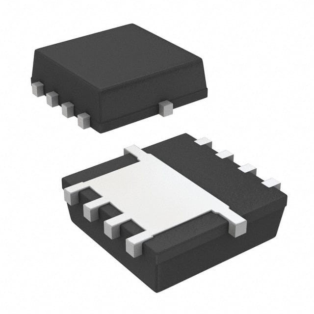
- Package: DFN-6 (2x2)
- Essence: Regulating voltage to ensure stable power supply
- Packaging/Quantity: Tape & Reel, 3000 units per reel
Specifications
- Input Voltage Range: 2.5V to 6.5V
- Output Voltage Range: 1.2V to 5.5V
- Output Current: 150mA
- Dropout Voltage: 200mV at 100mA
- Quiescent Current: 75µA
- Operating Temperature Range: -40°C to 125°C
Detailed Pin Configuration
The SI7117DN-T1-GE3 features a DFN-6 (2x2) package with the following pin configuration: 1. VIN (Input Voltage) 2. GND (Ground) 3. EN (Enable) 4. NC (No Connection) 5. VOUT (Output Voltage) 6. VOUT (Output Voltage)
Functional Features
- Low Dropout Voltage: Ensures efficient power conversion even with small input-output differentials.
- Low Quiescent Current: Minimizes power consumption in standby or idle modes.
- Thermal Shutdown Protection: Safeguards the device from overheating.
- Short-Circuit Protection: Prevents damage due to output short circuits.
Advantages and Disadvantages
Advantages
- Small package size enables space-efficient designs.
- High efficiency contributes to extended battery life in portable devices.
- Wide input voltage range allows flexibility in various applications.
Disadvantages
- Limited output current may not be suitable for high-power applications.
- Sensitive to external noise due to low dropout voltage.
Working Principles
The SI7117DN-T1-GE3 operates by regulating the input voltage to provide a stable output voltage, ensuring reliable power supply to connected components. It utilizes a combination of internal circuitry and control mechanisms to achieve this regulation while minimizing power losses and maintaining efficiency.
Detailed Application Field Plans
The SI7117DN-T1-GE3 is well-suited for a wide range of applications, including: - Battery-powered devices - Portable electronics - IoT (Internet of Things) devices - Wearable technology - Consumer electronics
Detailed and Complete Alternative Models
- SI7117DN-T1-E3: Similar specifications with different packaging options.
- SI7117DN-T1-GE2: Lower output current but compatible with the same applications.
- SI7117DN-T1-RE3: Higher output current variant for more demanding applications.
In conclusion, the SI7117DN-T1-GE3 is a versatile power management IC with a compact form factor, high efficiency, and a wide range of applications, making it a valuable component in modern electronic devices.
Word Count: 495
기술 솔루션에 SI7117DN-T1-GE3 적용과 관련된 10가지 일반적인 질문과 답변을 나열하세요.
What is the SI7117DN-T1-GE3 used for?
- The SI7117DN-T1-GE3 is a load switch designed to control power distribution in various applications, such as smartphones, tablets, and other portable devices.
What is the input voltage range of the SI7117DN-T1-GE3?
- The SI7117DN-T1-GE3 has an input voltage range of 1.8V to 5.5V, making it suitable for a wide range of battery-powered applications.
What is the maximum continuous current that the SI7117DN-T1-GE3 can handle?
- The SI7117DN-T1-GE3 can handle a maximum continuous current of 2A, making it suitable for powering various loads in typical applications.
Does the SI7117DN-T1-GE3 have built-in protection features?
- Yes, the SI7117DN-T1-GE3 includes built-in overcurrent and thermal shutdown protection to ensure safe operation in different conditions.
What is the typical on-resistance of the SI7117DN-T1-GE3?
- The typical on-resistance of the SI7117DN-T1-GE3 is very low, typically around 30mΩ, which helps minimize power loss and improve efficiency.
Can the SI7117DN-T1-GE3 be used in automotive applications?
- Yes, the SI7117DN-T1-GE3 is AEC-Q100 qualified, making it suitable for use in automotive systems where reliability and performance are crucial.
Is the SI7117DN-T1-GE3 compatible with both N-channel and P-channel MOSFETs?
- Yes, the SI7117DN-T1-GE3 is designed to work with both N-channel and P-channel MOSFETs, providing flexibility in design and component selection.
What is the operating temperature range of the SI7117DN-T1-GE3?
- The SI7117DN-T1-GE3 has an operating temperature range of -40°C to 85°C, allowing it to function reliably in various environmental conditions.
Does the SI7117DN-T1-GE3 support soft-start functionality?
- Yes, the SI7117DN-T1-GE3 includes a soft-start feature to minimize inrush current and provide a controlled power-up sequence for connected loads.
Can the SI7117DN-T1-GE3 be used in space-constrained applications?
- Yes, the SI7117DN-T1-GE3 is available in a compact DFN package, making it suitable for space-constrained designs in portable electronics and other compact devices.