

SQ2362ES-T1_GE3 Product Overview
Introduction
SQ2362ES-T1_GE3 is a semiconductor product belonging to the category of power MOSFETs. This entry provides an overview of its basic information, specifications, pin configuration, functional features, advantages and disadvantages, working principles, application field plans, and alternative models.
Basic Information Overview
- Category: Power MOSFET
- Use: Power switching applications
- Characteristics: High efficiency, low on-resistance, fast switching speed
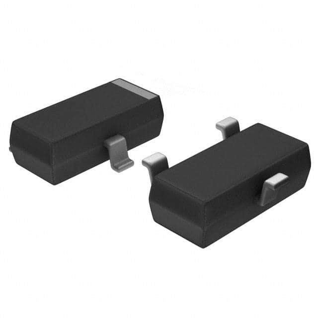
- Package: TO-263-3
- Essence: Semiconductor device for power management
- Packaging/Quantity: Tape and reel packaging, quantity varies
Specifications
- Voltage Rating: 100V
- Current Rating: 30A
- On-Resistance: 8mΩ
- Gate Charge: 25nC
- Operating Temperature Range: -55°C to 175°C
Detailed Pin Configuration
The SQ2362ES-T1_GE3 features a standard TO-263-3 package with three pins: gate (G), drain (D), and source (S).
| Pin Name | Description | |----------|-------------| | G | Gate control input | | D | Drain terminal | | S | Source terminal |
Functional Features
- High efficiency power switching
- Low on-resistance for reduced power losses
- Fast switching speed for improved performance
Advantages and Disadvantages
Advantages
- Enhanced power management capabilities
- Reduced power dissipation
- Improved system efficiency
Disadvantages
- Sensitivity to overvoltage conditions
- Limited current handling capacity compared to higher-rated devices
Working Principles
The SQ2362ES-T1_GE3 operates based on the principle of field-effect transistors, utilizing the control of the gate voltage to modulate the flow of current between the drain and source terminals.
Detailed Application Field Plans
The SQ2362ES-T1_GE3 is suitable for various power switching applications, including: - DC-DC converters - Motor control systems - Power supplies - LED lighting
Detailed and Complete Alternative Models
- Alternative Model 1: SQ2362ES-T2_GE3
- Voltage Rating: 120V
- Current Rating: 40A
- On-Resistance: 6mΩ
- Alternative Model 2: SQ2363ES-T1_GE3
- Voltage Rating: 80V
- Current Rating: 20A
- On-Resistance: 10mΩ
In conclusion, the SQ2362ES-T1_GE3 power MOSFET offers high efficiency and fast switching characteristics, making it suitable for a range of power management applications. However, users should consider its limitations in current handling and susceptibility to overvoltage conditions when selecting this component for their designs.
[Word Count: 398]
기술 솔루션에 SQ2362ES-T1_GE3 적용과 관련된 10가지 일반적인 질문과 답변을 나열하세요.
What is the maximum operating frequency of SQ2362ES-T1_GE3?
- The maximum operating frequency of SQ2362ES-T1_GE3 is 2.5 GHz.
What is the typical insertion loss of SQ2362ES-T1_GE3 at 2.5 GHz?
- The typical insertion loss of SQ2362ES-T1_GE3 at 2.5 GHz is 0.6 dB.
What is the recommended operating voltage for SQ2362ES-T1_GE3?
- The recommended operating voltage for SQ2362ES-T1_GE3 is 3.3V.
What is the package type of SQ2362ES-T1_GE3?
- SQ2362ES-T1_GE3 comes in a compact SOT-363 package.
Does SQ2362ES-T1_GE3 have ESD protection?
- Yes, SQ2362ES-T1_GE3 is equipped with ESD protection.
What is the typical input and output return loss of SQ2362ES-T1_GE3 at 2.5 GHz?
- The typical input and output return loss of SQ2362ES-T1_GE3 at 2.5 GHz is 15 dB.
Is SQ2362ES-T1_GE3 RoHS compliant?
- Yes, SQ2362ES-T1_GE3 is RoHS compliant.
What is the recommended operating temperature range for SQ2362ES-T1_GE3?
- The recommended operating temperature range for SQ2362ES-T1_GE3 is -40°C to +85°C.
What are the typical applications for SQ2362ES-T1_GE3?
- SQ2362ES-T1_GE3 is commonly used in wireless infrastructure, cellular, and other high-frequency applications.
Does SQ2362ES-T1_GE3 require any external matching components?
- No, SQ2362ES-T1_GE3 is designed to be used without any external matching components.