

XC2S150-6FGG456C
Product Overview
Category
XC2S150-6FGG456C belongs to the category of Field Programmable Gate Arrays (FPGAs).
Use
FPGAs are integrated circuits that can be programmed and reprogrammed to perform various digital functions. They are widely used in industries such as telecommunications, automotive, aerospace, and consumer electronics.
Characteristics
XC2S150-6FGG456C is a high-performance FPGA with advanced features. It offers flexibility, scalability, and reconfigurability, making it suitable for a wide range of applications.
Package
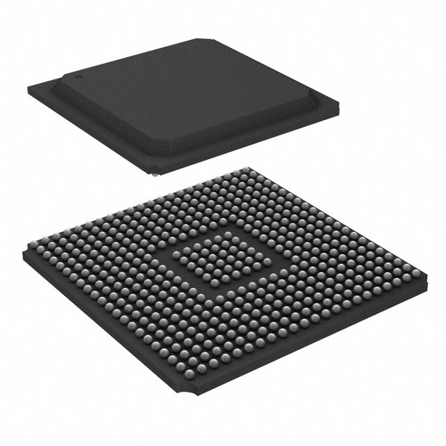
XC2S150-6FGG456C comes in a 456-ball Fine-Pitch Ball Grid Array (FBGA) package.
Essence
The essence of XC2S150-6FGG456C lies in its ability to provide a customizable hardware solution that can be tailored to specific requirements without the need for costly and time-consuming custom chip design.
Packaging/Quantity
XC2S150-6FGG456C is typically sold individually or in small quantities, depending on the customer's needs.
Specifications
- Device Type: FPGA
- Family: Spartan-II
- Number of Logic Cells: 150,000
- Number of I/Os: 456
- Operating Voltage: 3.3V
- Speed Grade: -6
- Package Type: FBGA
- Package Pins: 456
Detailed Pin Configuration
The detailed pin configuration of XC2S150-6FGG456C can be found in the product datasheet provided by the manufacturer.
Functional Features
XC2S150-6FGG456C offers several functional features that enhance its performance and versatility:
- High Logic Capacity: With 150,000 logic cells, it can handle complex digital designs.
- Flexible I/O Options: The 456 I/O pins provide ample connectivity options for interfacing with external devices.
- Reconfigurability: The FPGA can be reprogrammed on-the-fly, allowing for dynamic changes to the hardware design.
- Embedded Memory: XC2S150-6FGG456C includes embedded memory blocks that can be used for data storage or as lookup tables.
- Built-in DSP Blocks: The FPGA features dedicated Digital Signal Processing (DSP) blocks for efficient signal processing tasks.
Advantages and Disadvantages
Advantages
- Flexibility: FPGAs offer the ability to adapt to changing requirements without the need for hardware redesign.
- Time-to-Market: Using FPGAs can significantly reduce development time compared to custom chip design.
- Cost-Effective: FPGAs eliminate the need for expensive mask sets and allow for lower production costs.
Disadvantages
- Power Consumption: FPGAs generally consume more power compared to application-specific integrated circuits (ASICs).
- Complexity: Designing for FPGAs requires specialized knowledge and tools, which may increase development complexity.
Working Principles
XC2S150-6FGG456C operates based on the principles of configurable logic. It consists of an array of programmable logic cells interconnected by a network of configurable routing resources. The logic cells can be programmed to implement various digital functions, and the routing resources enable the interconnection of these cells to create complex circuits.
Detailed Application Field Plans
XC2S150-6FGG456C finds applications in various fields, including:
- Telecommunications: Used in base stations, routers, and network switches for high-speed data processing.
- Automotive: Employed in advanced driver-assistance systems (ADAS), infotainment systems, and engine control units.
- Aerospace: Utilized in satellite communication systems, avionics, and flight control systems.
- Consumer Electronics: Found in smart TVs, gaming consoles, and wearable devices for enhanced functionality.
Detailed and Complete Alternative Models
- XC2S50-6FGG456C: A lower-capacity version of the same FPGA family with 50,000 logic cells.
- XC2S200-6FGG456C: A higher-capacity version of the same FPGA family with 200,000 logic cells.
- XC2S300-6FGG456C: Another higher-capacity option with 300,000 logic cells.
These alternative models provide different levels of logic capacity to suit varying application requirements.
In conclusion, XC2S150-6FGG456C is a high-performance FPGA that offers flexibility, scalability, and reconfigurability. It finds applications in various industries and provides a customizable hardware solution without the need for custom chip design. While it has advantages such as flexibility and reduced time-to-market, it also has disadvantages like increased power consumption and complexity. Overall, XC2S150-6FGG456C is a versatile FPGA suitable for a wide range of digital applications.
기술 솔루션에 XC2S150-6FGG456C 적용과 관련된 10가지 일반적인 질문과 답변을 나열하세요.
Sure! Here are 10 common questions and answers related to the application of XC2S150-6FGG456C in technical solutions:
Question: What is XC2S150-6FGG456C?
- Answer: XC2S150-6FGG456C is a specific model of Field Programmable Gate Array (FPGA) manufactured by Xilinx.Question: What is the purpose of using XC2S150-6FGG456C in technical solutions?
- Answer: XC2S150-6FGG456C is used to implement digital logic circuits and perform complex computations in various technical applications.Question: What are some typical applications of XC2S150-6FGG456C?
- Answer: XC2S150-6FGG456C can be used in applications such as telecommunications, automotive systems, industrial automation, aerospace, and defense.Question: How does XC2S150-6FGG456C differ from other FPGAs?
- Answer: XC2S150-6FGG456C offers a specific combination of features, including a certain number of logic cells, I/O pins, and performance capabilities, which may vary from other FPGA models.Question: What are the key specifications of XC2S150-6FGG456C?
- Answer: Some key specifications include 150,000 system gates, 456-ball Fine-Pitch Ball Grid Array (FBGA) package, and a maximum operating frequency of 6 MHz.Question: Can XC2S150-6FGG456C be reprogrammed after deployment?
- Answer: Yes, XC2S150-6FGG456C is a programmable device, allowing for reconfiguration and updates to the implemented logic circuits.Question: What development tools are available for programming XC2S150-6FGG456C?
- Answer: Xilinx provides software tools like Vivado Design Suite, ISE Design Suite, and SDK (Software Development Kit) to program and configure XC2S150-6FGG456C.Question: Are there any limitations or considerations when using XC2S150-6FGG456C?
- Answer: Some considerations include power consumption, heat dissipation, I/O voltage compatibility, and the need for proper signal integrity measures in high-speed applications.Question: Can XC2S150-6FGG456C be used in safety-critical systems?
- Answer: Yes, XC2S150-6FGG456C can be used in safety-critical systems, but additional design and verification processes may be required to meet specific safety standards.Question: Where can I find more information about XC2S150-6FGG456C and its application in technical solutions?
- Answer: You can refer to Xilinx's official website, datasheets, application notes, and user guides for detailed information on XC2S150-6FGG456C and its application in various technical solutions.