

XC2S400E-6FGG456C
Product Overview
Category
XC2S400E-6FGG456C belongs to the category of Field Programmable Gate Arrays (FPGAs).
Use
FPGAs are integrated circuits that can be programmed and reprogrammed to perform various digital functions. They are widely used in industries such as telecommunications, automotive, aerospace, and consumer electronics.
Characteristics
XC2S400E-6FGG456C is known for its high performance, flexibility, and reconfigurability. It offers a large number of configurable logic blocks, memory elements, and I/O pins, allowing designers to implement complex digital systems.
Package
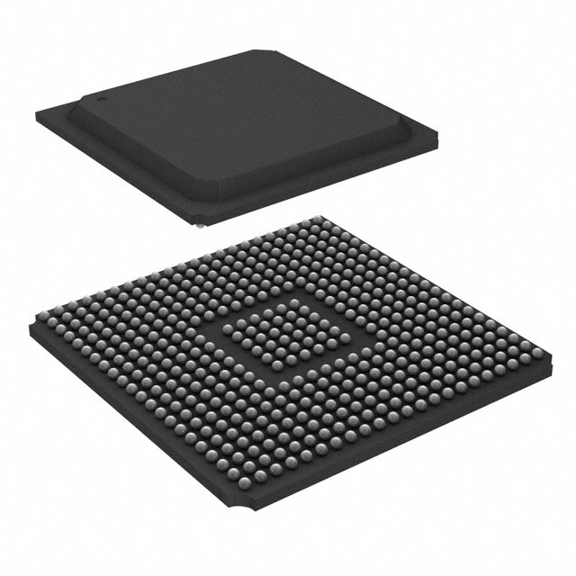
XC2S400E-6FGG456C comes in a Fine-Pitch Ball Grid Array (FBGA) package. This package provides a compact form factor and excellent thermal performance.
Essence
The essence of XC2S400E-6FGG456C lies in its ability to provide a customizable hardware platform for implementing digital designs. It allows designers to create highly optimized solutions for specific applications.
Packaging/Quantity
XC2S400E-6FGG456C is typically packaged in reels or trays, depending on the manufacturer's specifications. The quantity per package varies but is usually in the range of 100 to 1000 units.
Specifications
- Device Type: FPGA
- Family: Spartan-II
- Series: XC2S
- Logic Cells: 400,000
- Speed Grade: -6
- Package: FBGA
- Pin Count: 456
- Operating Voltage: 3.3V
- Maximum Operating Frequency: 200 MHz
- Configuration Memory: 4 Mb
- I/O Standards: LVCMOS, LVTTL, HSTL, SSTL, LVDS
Detailed Pin Configuration
The detailed pin configuration of XC2S400E-6FGG456C can be found in the manufacturer's datasheet. It provides information on the function and connectivity of each pin, allowing designers to properly interface with the FPGA.
Functional Features
XC2S400E-6FGG456C offers several functional features that make it a versatile choice for digital design:
- High Logic Capacity: With 400,000 logic cells, it can accommodate complex designs.
- Flexible I/O Options: The FPGA supports various I/O standards, enabling seamless integration with different devices.
- Reconfigurability: The ability to reprogram the FPGA allows for iterative design improvements and adaptability to changing requirements.
- Embedded Memory: The built-in memory elements provide efficient storage for data processing.
- Clock Management: The FPGA includes dedicated clock management resources for precise timing control.
Advantages and Disadvantages
Advantages
- Customizability: FPGAs offer the advantage of creating tailored solutions for specific applications.
- Rapid Prototyping: The reprogrammable nature of FPGAs allows for quick development and testing of digital designs.
- Cost-Effective: FPGAs eliminate the need for custom ASICs, reducing development costs for low-to-medium volume production.
Disadvantages
- Power Consumption: FPGAs tend to consume more power compared to fixed-function integrated circuits.
- Complexity: Designing with FPGAs requires specialized knowledge and expertise.
- Limited Performance: FPGAs may not match the performance of dedicated hardware for certain applications.
Working Principles
XC2S400E-6FGG456C operates based on the principles of configurable logic. It consists of an array of programmable logic blocks interconnected through configurable routing resources. The logic blocks can be programmed to implement desired digital functions, while the routing resources allow for the interconnection of these blocks.
The FPGA is programmed using a Hardware Description Language (HDL) such as VHDL or Verilog. The HDL code describes the desired functionality, which is then synthesized and mapped onto the FPGA's resources. Once programmed, the FPGA can execute the specified digital functions.
Detailed Application Field Plans
XC2S400E-6FGG456C finds applications in various fields, including:
- Telecommunications: FPGAs are used in base stations, routers, and network switches to handle high-speed data processing and protocol conversion.
- Automotive: FPGAs are employed in automotive electronics for functions like engine control, advanced driver-assistance systems (ADAS), and infotainment systems.
- Aerospace: FPGAs are utilized in satellite communication systems, avionics, and radar systems for their reliability and radiation tolerance.
- Consumer Electronics: FPGAs are integrated into devices like gaming consoles, high-definition televisions, and audio/video processing equipment to enable advanced features and customization.
Detailed and Complete Alternative Models
There are several alternative models available in the market that offer similar capabilities to XC2S400E-6FGG456
기술 솔루션에 XC2S400E-6FGG456C 적용과 관련된 10가지 일반적인 질문과 답변을 나열하세요.
Sure! Here are 10 common questions and answers related to the application of XC2S400E-6FGG456C in technical solutions:
Question: What is XC2S400E-6FGG456C?
Answer: XC2S400E-6FGG456C is a specific model of Field-Programmable Gate Array (FPGA) manufactured by Xilinx.Question: What are the key features of XC2S400E-6FGG456C?
Answer: Some key features of XC2S400E-6FGG456C include 400,000 system gates, 456-pin Fine-Pitch Ball Grid Array (FBGA) package, and support for various I/O standards.Question: What are the typical applications of XC2S400E-6FGG456C?
Answer: XC2S400E-6FGG456C can be used in a wide range of applications such as digital signal processing, telecommunications, industrial control systems, and high-performance computing.Question: How does XC2S400E-6FGG456C differ from other FPGAs?
Answer: XC2S400E-6FGG456C offers a balance between cost, performance, and power consumption, making it suitable for many general-purpose applications.Question: Can XC2S400E-6FGG456C be reprogrammed after deployment?
Answer: Yes, XC2S400E-6FGG456C is a reprogrammable FPGA, allowing for flexibility in design iterations and updates.Question: What development tools are available for programming XC2S400E-6FGG456C?
Answer: Xilinx provides software tools like Vivado Design Suite that enable designers to program and configure XC2S400E-6FGG456C.Question: What is the power consumption of XC2S400E-6FGG456C?
Answer: The power consumption of XC2S400E-6FGG456C depends on the specific design and operating conditions, but it is generally designed to be power-efficient.Question: Can XC2S400E-6FGG456C interface with other components or devices?
Answer: Yes, XC2S400E-6FGG456C supports various I/O standards, allowing it to interface with different components and devices in a system.Question: Are there any limitations or considerations when using XC2S400E-6FGG456C?
Answer: Some considerations include understanding the FPGA's capabilities, managing power requirements, and ensuring proper signal integrity in the design.Question: Where can I find more information about XC2S400E-6FGG456C?
Answer: You can refer to Xilinx's official documentation, datasheets, and application notes for detailed information about XC2S400E-6FGG456C and its application in technical solutions.
Please note that the answers provided here are general and may vary based on specific requirements and use cases. It is always recommended to consult the manufacturer's documentation and seek expert advice for your specific application.