

XC2V1000-6BGG575C
Product Overview
Category
The XC2V1000-6BGG575C belongs to the category of Field Programmable Gate Arrays (FPGAs).
Use
FPGAs are integrated circuits that can be programmed and reprogrammed to perform various digital functions. The XC2V1000-6BGG575C is specifically designed for high-performance applications requiring complex logic functions.
Characteristics
- High-density programmable logic device
- Advanced architecture for efficient performance
- Flexible and customizable design
- Wide range of I/O options
- Low power consumption
- Fast processing speed
Package
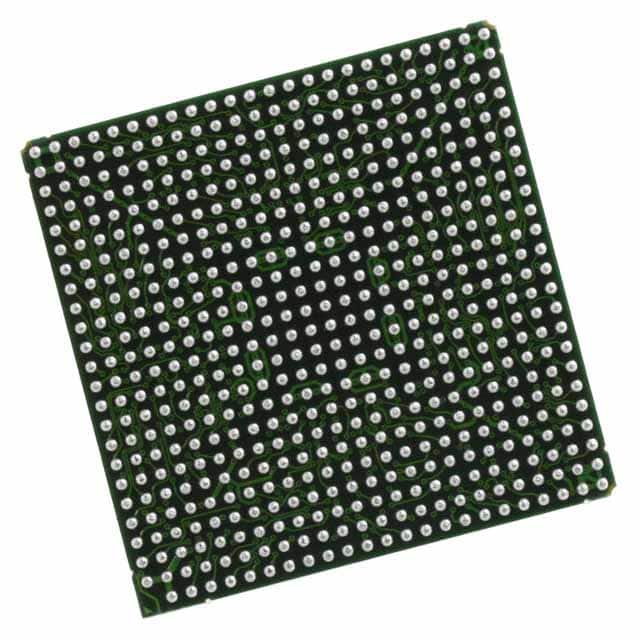
The XC2V1000-6BGG575C comes in a Ball Grid Array (BGA) package.
Essence
The essence of the XC2V1000-6BGG575C lies in its ability to provide a versatile and powerful platform for implementing complex digital designs.
Packaging/Quantity
The XC2V1000-6BGG575C is typically packaged individually and is available in various quantities depending on the manufacturer's specifications.
Specifications
- Device Type: FPGA
- Logic Cells: 1,000
- Speed Grade: -6
- Package Type: BGA
- Package Pins: 575
- Operating Voltage: 3.3V
- Maximum Frequency: 200 MHz
- I/O Standards: LVCMOS, LVTTL, HSTL, SSTL, LVDS, etc.
- Configuration Memory: Flash or SRAM-based
Detailed Pin Configuration
The XC2V1000-6BGG575C has 575 pins arranged in a specific configuration. Please refer to the datasheet provided by the manufacturer for detailed pin assignments.
Functional Features
- High-speed data processing capabilities
- Configurable logic blocks for custom designs
- Built-in memory blocks for efficient data storage
- Dedicated input/output pins for interfacing with external devices
- Clock management resources for precise timing control
- On-chip programmable interconnects for flexible routing
Advantages and Disadvantages
Advantages
- Versatile and customizable design options
- High-performance capabilities
- Low power consumption compared to traditional ASICs
- Faster time-to-market due to reprogrammability
- Cost-effective solution for prototyping and low-volume production
Disadvantages
- Limited scalability compared to Application-Specific Integrated Circuits (ASICs)
- Higher cost per unit compared to mass-produced ASICs
- Design complexity may require specialized knowledge and tools
Working Principles
The XC2V1000-6BGG575C operates based on the principles of configurable logic. It consists of a matrix of programmable logic cells interconnected through programmable routing resources. The device can be programmed using Hardware Description Languages (HDL) such as VHDL or Verilog, which define the desired functionality of the circuit. Once programmed, the FPGA executes the specified logic functions.
Detailed Application Field Plans
The XC2V1000-6BGG575C finds applications in various fields, including:
- Telecommunications: Used in base stations, network routers, and communication equipment for signal processing and protocol handling.
- Aerospace and Defense: Employed in radar systems, avionics, and military-grade communication systems for high-speed data processing and encryption.
- Industrial Automation: Utilized in control systems, robotics, and machine vision applications for real-time data processing and control.
- Medical Devices: Integrated into medical imaging equipment, patient monitoring systems, and diagnostic instruments for high-performance data processing.
- Automotive: Applied in advanced driver assistance systems (ADAS), infotainment systems, and engine control units for efficient data processing and control.
Detailed and Complete Alternative Models
- XC7A100T-2FGG484C: A newer generation FPGA with higher logic capacity and improved performance.
- EP4CE10F17C8N: An alternative FPGA from a different manufacturer, offering similar features and capabilities.
- Lattice iCE40UP5K-SG48I: A low-power FPGA suitable for battery-operated devices and IoT applications.
These alternative models provide options with varying specifications and price points, allowing users to choose the most suitable FPGA for their specific requirements.
Word count: 570 words
기술 솔루션에 XC2V1000-6BGG575C 적용과 관련된 10가지 일반적인 질문과 답변을 나열하세요.
Sure! Here are 10 common questions and answers related to the application of XC2V1000-6BGG575C in technical solutions:
Q: What is XC2V1000-6BGG575C? A: XC2V1000-6BGG575C is a field-programmable gate array (FPGA) manufactured by Xilinx. It is designed for high-performance applications and offers 1000 logic cells.
Q: What are the key features of XC2V1000-6BGG575C? A: Some key features include 1000 logic cells, 575-ball grid array (BGA) package, 6ns maximum delay, 5V tolerant I/Os, and 3.3V core voltage.
Q: What are the typical applications of XC2V1000-6BGG575C? A: XC2V1000-6BGG575C can be used in various applications such as digital signal processing, telecommunications, industrial control systems, automotive electronics, and aerospace.
Q: How does XC2V1000-6BGG575C differ from other FPGAs? A: XC2V1000-6BGG575C stands out with its specific combination of logic cells, package type, speed, and voltage tolerance. It offers a balance between performance and cost-effectiveness.
Q: Can XC2V1000-6BGG575C be reprogrammed after deployment? A: Yes, XC2V1000-6BGG575C is a field-programmable device, meaning it can be reprogrammed even after it has been deployed in a system.
Q: What development tools are available for programming XC2V1000-6BGG575C? A: Xilinx provides various development tools like Vivado Design Suite and ISE Design Suite, which offer a comprehensive environment for designing, simulating, and programming XC2V1000-6BGG575C.
Q: Can XC2V1000-6BGG575C interface with other components or devices? A: Yes, XC2V1000-6BGG575C supports various communication protocols such as SPI, I2C, UART, and Ethernet, allowing it to interface with other components or devices in a system.
Q: What is the power consumption of XC2V1000-6BGG575C? A: The power consumption of XC2V1000-6BGG575C depends on the design and utilization. It is recommended to refer to the datasheet and use power estimation tools provided by Xilinx.
Q: Are there any limitations or considerations when using XC2V1000-6BGG575C? A: Some considerations include the available logic resources, I/O count, power requirements, and thermal management. It is important to carefully plan and optimize the design to meet the requirements.
Q: Where can I find additional resources and support for XC2V1000-6BGG575C? A: Xilinx's website provides extensive documentation, application notes, user guides, and forums where you can find additional resources and get support for XC2V1000-6BGG575C.