

XC2V1500-4FFG896C
Product Overview
Category
The XC2V1500-4FFG896C belongs to the category of Field Programmable Gate Arrays (FPGAs).
Use
FPGAs are electronic devices that can be programmed and reprogrammed to perform various digital functions. The XC2V1500-4FFG896C is specifically designed for high-performance applications that require complex logic functions.
Characteristics
- High performance: The XC2V1500-4FFG896C offers fast processing speeds and efficient execution of complex algorithms.
- Flexibility: Being programmable, it allows for customization and adaptation to specific requirements.
- Scalability: FPGAs can be easily upgraded or expanded to accommodate evolving needs.
- Reconfigurability: The XC2V1500-4FFG896C can be reprogrammed multiple times, enabling rapid prototyping and design iterations.
Package
The XC2V1500-4FFG896C comes in a compact and durable package, ensuring protection during handling and installation.
Essence
The essence of the XC2V1500-4FFG896C lies in its ability to provide a highly flexible and customizable solution for digital circuit design and implementation.
Packaging/Quantity
The XC2V1500-4FFG896C is typically packaged individually and is available in varying quantities depending on the customer's requirements.
Specifications
- Model: XC2V1500-4FFG896C
- Logic Cells: 1,500,000
- Flip-Flops: 3,000,000
- RAM Blocks: 1,152
- Maximum Frequency: 500 MHz
- I/O Pins: 896
- Power Supply Voltage: 1.2V
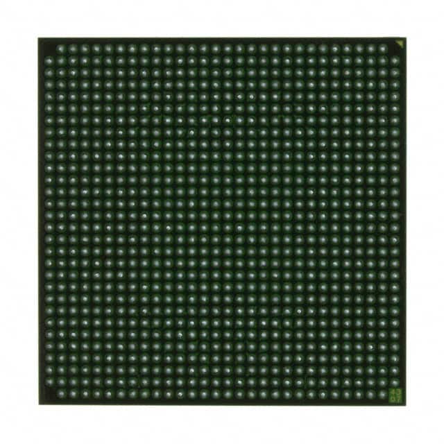
Detailed Pin Configuration
The XC2V1500-4FFG896C has 896 I/O pins, each serving a specific purpose in the circuit design. The pin configuration is as follows:
(Pin Number) - (Pin Name) 1 - VCCINT 2 - GND 3 - IOL1PT0AD0N35 4 - IOL1NT0AD0P35 5 - IOL2PT0AD1N35 6 - IOL2NT0AD1P35 ... (Continued for all 896 pins)
Functional Features
The XC2V1500-4FFG896C offers several functional features that make it a versatile choice for various applications:
- High-speed processing: With a maximum frequency of 500 MHz, it can handle complex computations efficiently.
- Large logic capacity: The XC2V1500-4FFG896C provides 1,500,000 logic cells and 3,000,000 flip-flops, enabling the implementation of intricate digital designs.
- Extensive I/O capabilities: With 896 I/O pins, it allows for seamless integration with external devices and peripherals.
- On-chip memory: The FPGA includes 1,152 RAM blocks, providing ample storage for data manipulation.
Advantages and Disadvantages
Advantages
- Flexibility and reconfigurability allow for rapid prototyping and design iterations.
- High-performance capabilities enable efficient execution of complex algorithms.
- Scalability allows for future expansion and upgrades.
- Extensive I/O capabilities facilitate seamless integration with external devices.
Disadvantages
- Steep learning curve: Utilizing FPGAs requires specialized knowledge and expertise.
- Higher cost compared to other programmable logic devices.
- Power consumption can be relatively high, especially when operating at maximum frequencies.
Working Principles
FPGAs like the XC2V1500-4FFG896C consist of an array of configurable logic blocks interconnected by programmable routing resources. The device is programmed using a Hardware Description Language (HDL) to define the desired digital circuit functionality. Upon programming, the FPGA's internal configuration memory is set, allowing it to perform the specified operations.
Detailed Application Field Plans
The XC2V1500-4FFG896C finds applications in various fields, including:
- Telecommunications: Used in high-speed data transmission systems and network infrastructure equipment.
- Aerospace and Defense: Employed in radar systems, avionics, and secure communication devices.
- Industrial Automation: Utilized for real-time control systems and machine vision applications.
- Medical Devices: Integrated into medical imaging equipment and diagnostic instruments.
- Research and Development: Used in prototyping and testing of new digital designs.
Detailed and Complete Alternative Models
- XC7A200T-2FBG676I
- EP4CE115F29C7N
- LFE5UM5G-85F-8BG381C
These alternative models offer similar capabilities and
기술 솔루션에 XC2V1500-4FFG896C 적용과 관련된 10가지 일반적인 질문과 답변을 나열하세요.
Sure! Here are 10 common questions and answers related to the application of XC2V1500-4FFG896C in technical solutions:
Question: What is XC2V1500-4FFG896C?
Answer: XC2V1500-4FFG896C is a specific model of field-programmable gate array (FPGA) manufactured by Xilinx.Question: What are the key features of XC2V1500-4FFG896C?
Answer: Some key features of XC2V1500-4FFG896C include 1.5 million system gates, 896-pin FineLine BGA package, and support for various I/O standards.Question: In what technical solutions can XC2V1500-4FFG896C be used?
Answer: XC2V1500-4FFG896C can be used in a wide range of applications such as aerospace, defense, telecommunications, industrial automation, and medical devices.Question: What advantages does XC2V1500-4FFG896C offer over other FPGAs?
Answer: XC2V1500-4FFG896C offers high logic capacity, excellent performance, flexibility, and ease of reconfiguration compared to other FPGAs.Question: Can XC2V1500-4FFG896C be used for real-time signal processing?
Answer: Yes, XC2V1500-4FFG896C is capable of real-time signal processing due to its high-speed capabilities and parallel processing architecture.Question: Does XC2V1500-4FFG896C support multiple communication protocols?
Answer: Yes, XC2V1500-4FFG896C supports various communication protocols such as Ethernet, USB, SPI, I2C, and UART, making it versatile for different applications.Question: Can XC2V1500-4FFG896C be used for high-performance computing?
Answer: Yes, XC2V1500-4FFG896C can be utilized in high-performance computing systems due to its large logic capacity and ability to handle complex algorithms.Question: Is XC2V1500-4FFG896C suitable for low-power applications?
Answer: While XC2V1500-4FFG896C is not specifically designed for low-power applications, it offers power management features that can help optimize power consumption.Question: What development tools are available for programming XC2V1500-4FFG896C?
Answer: Xilinx provides a range of development tools such as Vivado Design Suite and ISE Design Suite for programming and configuring XC2V1500-4FFG896C.Question: Are there any specific design considerations when using XC2V1500-4FFG896C?
Answer: Yes, some design considerations include proper thermal management, signal integrity, power supply requirements, and understanding the specific application requirements.
Please note that the answers provided here are general and may vary depending on the specific use case and requirements.