

XC2V1500-4FFG896I
Product Overview
Category
XC2V1500-4FFG896I belongs to the category of Field Programmable Gate Arrays (FPGAs).
Use
This product is primarily used in digital logic circuits and electronic systems for various applications.
Characteristics
- Programmable: The XC2V1500-4FFG896I can be reprogrammed to perform different functions, making it highly versatile.
- High Performance: It offers high-speed operation and efficient processing capabilities.
- Flexibility: The FPGA allows for customization and adaptation to specific requirements.
- Integration: It integrates multiple logic gates and components into a single chip, reducing the need for external components.
- Scalability: The XC2V1500-4FFG896I can be easily scaled up or down depending on the complexity of the design.
Package and Quantity
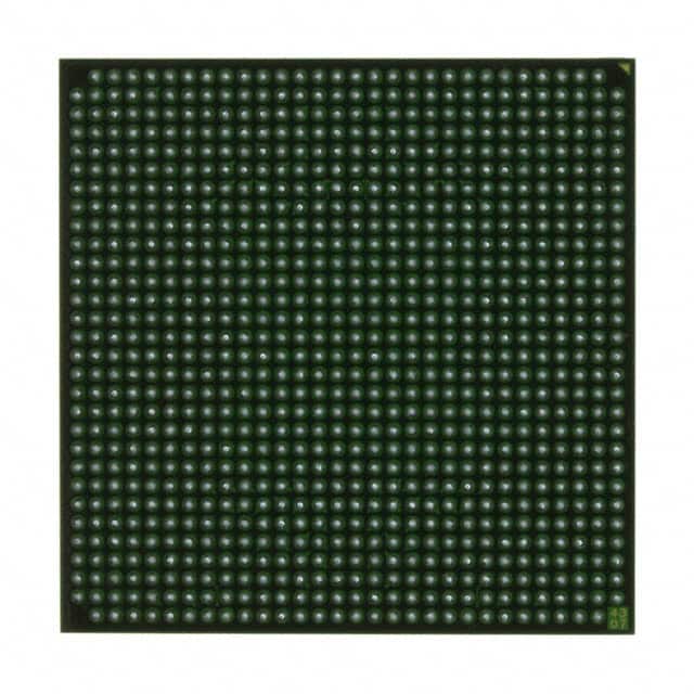
The XC2V1500-4FFG896I is available in a Fine-Pitch Ball Grid Array (FBGA) package. Each package contains one unit of the FPGA.
Specifications
- Model: XC2V1500-4FFG896I
- Logic Cells: 1,500,000
- Flip-Flops: 4,000
- RAM Blocks: 576
- Maximum Frequency: 400 MHz
- Operating Voltage: 1.2V
- I/O Pins: 896
- Package Type: FBGA
- Package Dimensions: 23mm x 23mm
Pin Configuration
The detailed pin configuration of the XC2V1500-4FFG896I can be found in the manufacturer's datasheet.
Functional Features
- Reconfigurability: The XC2V1500-4FFG896I can be dynamically reconfigured to adapt to changing requirements.
- Parallel Processing: It supports parallel processing, enabling faster execution of complex algorithms.
- On-Chip Memory: The FPGA includes embedded memory blocks for efficient data storage and retrieval.
- I/O Flexibility: The XC2V1500-4FFG896I offers a wide range of I/O options, allowing seamless integration with external devices.
- Low Power Consumption: It is designed to minimize power consumption while maintaining high performance.
Advantages and Disadvantages
Advantages
- Versatility: The reprogrammable nature of FPGAs allows for quick prototyping and design iterations.
- High Performance: The XC2V1500-4FFG896I offers fast processing speeds and efficient resource utilization.
- Integration: It eliminates the need for additional components, reducing system complexity and cost.
- Scalability: FPGAs can be easily scaled up or down to meet the requirements of different applications.
Disadvantages
- Complexity: Designing and programming FPGAs requires specialized knowledge and expertise.
- Cost: FPGAs can be more expensive compared to other programmable logic devices.
- Limited Resources: The available resources within an FPGA, such as logic cells and memory blocks, may impose constraints on the complexity of designs.
Working Principles
The XC2V1500-4FFG896I operates based on the principles of configurable logic. It consists of an array of programmable logic blocks interconnected by configurable routing channels. These logic blocks can be programmed to implement various digital functions, allowing for the creation of complex circuits. The configuration of the FPGA is stored in internal memory elements, which can be modified to change the behavior of the device.
Application Field Plans
The XC2V1500-4FFG896I finds applications in various fields, including: 1. Telecommunications: Used in network routers, switches, and base stations for high-speed data processing. 2. Aerospace and Defense: Employed in radar systems, avionics, and military communication equipment. 3. Industrial Automation: Used for control systems, robotics, and machine vision applications. 4. Medical Devices: Utilized in medical imaging, patient monitoring, and diagnostic equipment. 5. Automotive: Applied in advanced driver-assistance systems (ADAS), infotainment systems, and engine control units.
Alternative Models
- XC2V1000-4FFG896I: A lower-capacity version of the XC2V1500-4FFG896I with 1,000,000 logic cells.
- XC2V2000-4FFG896I: A higher-capacity version of the XC2V1500-4FFG896I with 2,000,000 logic cells.
- XC2V3000-4FFG896I: An even higher-capacity version of the XC2V1500-4FFG896I with 3,000,000 logic cells.
These alternative models offer different levels of capacity to suit varying project requirements.
In conclusion, the XC2V1500-4FFG
기술 솔루션에 XC2V1500-4FFG896I 적용과 관련된 10가지 일반적인 질문과 답변을 나열하세요.
Sure! Here are 10 common questions and answers related to the application of XC2V1500-4FFG896I in technical solutions:
Question: What is XC2V1500-4FFG896I?
Answer: XC2V1500-4FFG896I is a specific model of Field Programmable Gate Array (FPGA) manufactured by Xilinx.Question: What are the key features of XC2V1500-4FFG896I?
Answer: Some key features of XC2V1500-4FFG896I include 1,500,000 system gates, 896-pin FineLine BGA package, and support for various I/O standards.Question: In what technical solutions can XC2V1500-4FFG896I be used?
Answer: XC2V1500-4FFG896I can be used in a wide range of applications such as digital signal processing, high-performance computing, telecommunications, and aerospace.Question: What advantages does XC2V1500-4FFG896I offer over other FPGAs?
Answer: XC2V1500-4FFG896I offers high logic capacity, advanced performance, and flexibility due to its large number of system gates and configurable nature.Question: Can XC2V1500-4FFG896I be programmed using industry-standard design tools?
Answer: Yes, XC2V1500-4FFG896I can be programmed using Xilinx's Vivado Design Suite, which is an industry-standard tool for FPGA development.Question: What kind of I/O interfaces does XC2V1500-4FFG896I support?
Answer: XC2V1500-4FFG896I supports various I/O standards such as LVCMOS, LVTTL, HSTL, SSTL, and differential signaling standards like LVDS and LVPECL.Question: Can XC2V1500-4FFG896I be used in safety-critical applications?
Answer: Yes, XC2V1500-4FFG896I can be used in safety-critical applications as long as it is properly designed and validated to meet the required safety standards.Question: What kind of power supply does XC2V1500-4FFG896I require?
Answer: XC2V1500-4FFG896I requires a single 3.3V power supply for its core voltage, and additional voltages may be needed for I/O interfaces.Question: Can XC2V1500-4FFG896I be reprogrammed after deployment?
Answer: Yes, XC2V1500-4FFG896I is a field-programmable device, which means it can be reprogrammed even after it has been deployed in a system.Question: Are there any specific design considerations when using XC2V1500-4FFG896I?
Answer: Yes, some design considerations include proper thermal management, signal integrity, power supply decoupling, and adherence to Xilinx's guidelines for optimal performance.
Please note that these answers are general and may vary depending on the specific requirements and use cases of XC2V1500-4FFG896I in different technical solutions.