

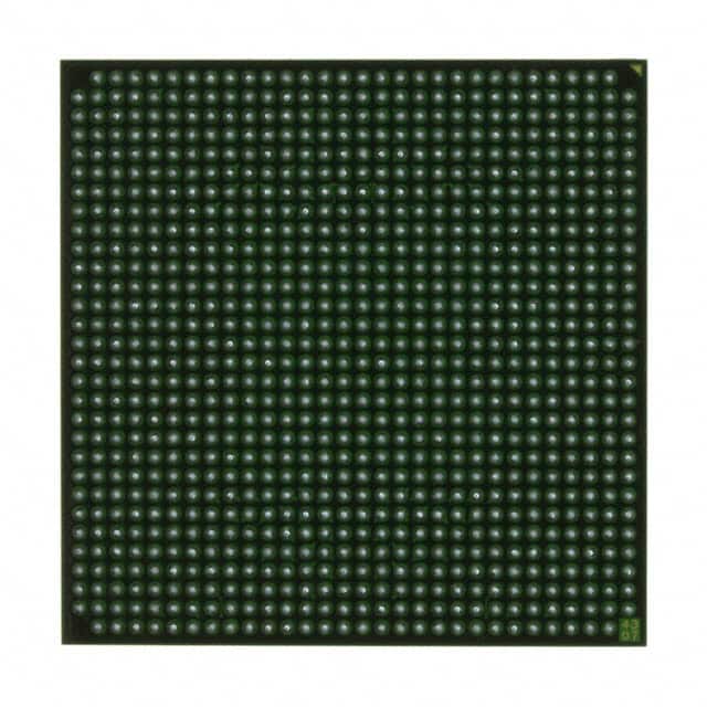
XC2V1500-5FFG896I
Product Overview
Category
The XC2V1500-5FFG896I belongs to the category of Field Programmable Gate Arrays (FPGAs).
Use
FPGAs are integrated circuits that can be programmed and reprogrammed to perform various digital functions. The XC2V1500-5FFG896I is specifically designed for high-performance applications that require complex logic operations.
Characteristics
- High-performance FPGA with advanced features
- Flexible and reconfigurable design
- Large number of programmable logic cells
- High-speed interconnects for efficient data transfer
- Support for various I/O standards
- On-chip memory resources for data storage
Package
The XC2V1500-5FFG896I comes in a compact package that ensures easy integration into electronic systems. It is designed to be mounted on a printed circuit board (PCB) using surface mount technology (SMT).
Essence
The essence of the XC2V1500-5FFG896I lies in its ability to provide customizable digital logic functionality, allowing designers to implement complex algorithms and processing tasks efficiently.
Packaging/Quantity
The XC2V1500-5FFG896I is typically packaged individually and is available in varying quantities depending on the manufacturer's specifications.
Specifications
- FPGA Family: Virtex-II
- Logic Cells: 1,500
- System Gates: 1,000,000
- Maximum Frequency: 400 MHz
- Number of I/O Pins: 896
- Operating Voltage: 3.3V
- Operating Temperature Range: -40°C to 100°C
Detailed Pin Configuration
The XC2V1500-5FFG896I has 896 I/O pins, each serving a specific purpose in the overall functionality of the FPGA. The pin configuration is detailed in the manufacturer's datasheet.
Functional Features
- High-speed data processing capabilities
- Configurable logic blocks for implementing complex algorithms
- On-chip memory resources for efficient data storage
- Support for various communication protocols and standards
- Flexible I/O options for interfacing with external devices
- Built-in clock management resources for precise timing control
Advantages and Disadvantages
Advantages
- Customizable and reprogrammable design allows for flexibility in system development
- High-performance capabilities enable efficient execution of complex tasks
- Large number of logic cells provide ample resources for implementing intricate algorithms
- Support for various I/O standards facilitates seamless integration with external devices
Disadvantages
- Higher cost compared to other programmable logic devices
- Steeper learning curve for designers unfamiliar with FPGA programming
- Limited availability of alternative models with similar specifications
Working Principles
The XC2V1500-5FFG896I operates based on the principles of digital logic. It consists of configurable logic blocks (CLBs) that can be programmed to perform specific functions. These CLBs are interconnected using a network of high-speed interconnects, allowing for efficient data transfer between different parts of the FPGA. The programmable nature of FPGAs enables designers to create custom digital circuits by configuring the logic elements and interconnections according to their requirements.
Detailed Application Field Plans
The XC2V1500-5FFG896I finds applications in various fields where high-performance digital processing is required. Some potential application areas include:
- Telecommunications: Implementing signal processing algorithms for wireless communication systems.
- Aerospace and Defense: Designing radar and sonar systems, image processing, and encryption algorithms.
- Industrial Automation: Controlling and monitoring complex manufacturing processes.
- Medical Imaging: Processing and analyzing medical images for diagnostic purposes.
- High-Frequency Trading: Implementing high-speed trading algorithms in financial markets.
Detailed and Complete Alternative Models
While the XC2V1500-5FFG896I offers advanced features and performance, there are alternative FPGA models available with similar capabilities. Some notable alternatives include:
- Xilinx Virtex-7 Series
- Intel (Altera) Stratix 10 Series
- Lattice Semiconductor ECP5 Series
- Microchip PolarFire Series
These alternative models provide a range of options for designers based on their specific requirements and preferences.
In conclusion, the XC2V1500-5FFG896I is a high-performance FPGA that offers flexibility, advanced features, and a large number of logic cells. Its customizable nature makes it suitable for various applications in telecommunications, aerospace, industrial automation, medical imaging, and high-frequency trading. While it has advantages such as reprogrammability and high-performance capabilities, it also has disadvantages like higher cost and limited availability of alternative models. Designers can consider alternative FPGA models based on their specific needs.
기술 솔루션에 XC2V1500-5FFG896I 적용과 관련된 10가지 일반적인 질문과 답변을 나열하세요.
Sure! Here are 10 common questions and answers related to the application of XC2V1500-5FFG896I in technical solutions:
Question: What is XC2V1500-5FFG896I?
Answer: XC2V1500-5FFG896I is a specific model of Field Programmable Gate Array (FPGA) manufactured by Xilinx.Question: What are the key features of XC2V1500-5FFG896I?
Answer: Some key features of XC2V1500-5FFG896I include 1,500,000 system gates, 896-pin FineLine BGA package, and support for various I/O standards.Question: In what technical solutions can XC2V1500-5FFG896I be used?
Answer: XC2V1500-5FFG896I can be used in a wide range of applications such as digital signal processing, high-performance computing, telecommunications, and aerospace.Question: What advantages does XC2V1500-5FFG896I offer over other FPGAs?
Answer: XC2V1500-5FFG896I offers high logic capacity, advanced performance, and flexibility due to its large number of system gates and configurable nature.Question: Can XC2V1500-5FFG896I be programmed using industry-standard design tools?
Answer: Yes, XC2V1500-5FFG896I can be programmed using Xilinx's Vivado Design Suite, which is an industry-standard tool for FPGA development.Question: Is XC2V1500-5FFG896I suitable for real-time applications?
Answer: Yes, XC2V1500-5FFG896I is capable of handling real-time applications due to its high-performance capabilities and low-latency design.Question: Can XC2V1500-5FFG896I be used in safety-critical systems?
Answer: Yes, XC2V1500-5FFG896I can be used in safety-critical systems as long as proper design practices and redundancy measures are implemented.Question: What is the power consumption of XC2V1500-5FFG896I?
Answer: The power consumption of XC2V1500-5FFG896I depends on the specific design and utilization, but it typically falls within a reasonable range for FPGA devices.Question: Are there any known limitations or constraints of XC2V1500-5FFG896I?
Answer: XC2V1500-5FFG896I may have limitations in terms of maximum clock frequency, available I/O pins, and resource utilization, which should be considered during the design phase.Question: Where can I find more information about XC2V1500-5FFG896I and its application in technical solutions?
Answer: You can refer to Xilinx's official documentation, datasheets, application notes, and online forums for more detailed information about XC2V1500-5FFG896I and its various applications.